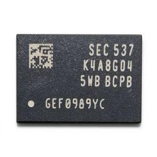
K4AAG085WM-BCRC - 32Gb DDR4 SDRAM x8 1.2V | Samsung
Артикул: K4AAG085WM-BCRC ✓ Активен| Кол-во | Цена за ед. | Итого |
|---|---|---|
| 1 | $1 | $1,00 |
| 10 | $1 | $10,00 |
| 100 | $1 | $100,00 |
| 500 | $1 | $500,00 |
| 1.000 | $1 | $1.000,00 |
K4AAG085WM-BCRC Обзор
DDR4 SDRAM (Double Data Rate 4 Synchronous Dynamic Random Access Memory) is the fourth generation of the DDR DRAM hierarchy: DRAM -> synchronous DRAM -> DDR SDRAM -> DDR4 SDRAM -> memory subsystem of a computing platform. Compared with DDR3, DDR4 lowers the core supply to 1.2V (about 25% lower power per Samsung), uses a bank-group architecture, and raises pre-fetch and data-rate limits, making it the dominant main-memory technology in servers, desktops, and embedded controllers.
Key family features include the 1.2V VDD supply with separate 1.2V VDDQ, on-die termination (ODT), bank-group architecture with up to 16 banks, programmable CAS latency, and a CRC/CA parity option on the command/address bus. The x8 organization simplifies layout versus x16 variants at equal density and matches ECC-native memory controllers. The -BCRC speed suffix denotes one of Samsung's DDR4 speed grades; the 'B' die/grade codes identify the fab process generation used by Samsung for its DDR4 lineup.
Technically, DDR4 SDRAM synchronizes all operations to a differential clock (CK/CK#) and transfers two data words per clock cycle on the DQ bus. Samsung's DDR4 devices integrate DLL-based output timing, a 1.2V SSTL12 I/O interface, and thermal features that support reliable operation in dense memory subsystems.
Typical applications include server DIMMs and memory-down designs on x86 and ARM platforms, industrial gateways, networking line cards, and FPGA-based processing boards that use DDR4 memory controllers.
Design consideration: always follow Samsung's layout guidance for length-matched, impedance-controlled DQ/CA routing (typically 40-ohm on-die-terminated nets) and verify the exact speed grade and CAS latency mapping of the -BCRC suffix in the official datasheet before finalizing the memory controller configuration.
This page synthesizes distributor stock data, same-family drop-in alternatives, and design notes not found in the manufacturer datasheet.
Аналоги без доработки для K4AAG085WM-BCRC — тот же корпус, pin-to-pin совместимость. Компоненты в других корпусах, требующие переработки PCB, исключены.
Варианты в этой серии
Модели той же серии, совместимые без доработки с K4AAG085WM-BCRC (тот же форм-фактор и посадочное место) — отличается по Package, Interface, Operating Temperature, Density, Data Rate.
Инструмент быстрого сравнения — выберите альтернативные компоненты для сравнения бок о бок:
K4AAG085WM-BCTD
✅ Прямая замена✓ В наличии
$9.95 / шт.
Открыть даташит →K4AAG085WA-BCRC
✅ Прямая замена ⚠️ Характеристики не проверены✓ В наличии
$6.1 / шт.
Открыть даташит →K4AAG085WA-BCWE
✅ Прямая замена ⚠️ Характеристики не проверены✓ В наличии
$7.24 / шт.
Открыть даташит →K4AAG085WA-BCTD
✅ Прямая замена ⚠️ Характеристики не проверены✓ В наличии
$10.18 / шт.
Открыть даташит →K4AAG085WA-BCPB
✅ Прямая замена ⚠️ Характеристики не проверены✓ В наличии
$6.92 / шт.
Открыть даташит →K4AAG085WM-BCRC Максимальные параметры и электрические характеристики
| Тип памяти | DDR4 SDRAM |
| Организация памяти | x8 |
| Supply Voltage (VDD) | 1.2 V |
| I/O Voltage (VDDQ) | 1.2 V |
| Max Data Rate | Up to 3200 Mbps/pin (family max per Samsung DDR4 page) |
| Интерфейс | SSTL12 |
| Корпус | 78-ball FBGA |
| Тип монтажа | Surface Mount |
| Architecture | Bank-group DDR4 |
| Termination | On-Die Termination (ODT) |
| Clock | Differential clock CK/CK# |
Руководство по цоколевке K4AAG085WM-BCRC в корпусе 78-ball fbga
Цоколевка для K4AAG085WM-BCRC (корпус 78-ball fbga). Эта цифровая ИС включает выводы GPIO, интерфейсы связи (UART, SPI, I2C) и выводы питания. Обратитесь к техническому описанию производителя для альтернативных функций выводов и вариантов конфигурации. Необходимо для проектирования встраиваемых систем и трассировки печатных плат.

Нет подробных данных о распиновке для K4AAG085WM-BCRC.
Обратитесь к даташиту для полной конфигурации выводов.
Типичное применение
K4AAG085WM-BCRC подходит для 6 применениеs: Server Main Memory (Memory-Down), Embedded Industrial Controllers, Networking Line Cards, FPGA Processing Boards, Desktop and Client Computing, Test and Measurement Instruments.
Server Main Memory (Memory-Down)
Server platforms require large, reliable main-memory arrays with ECC support. The K4AAG085WM-BCRC's x8 organization is the standard width for ECC computation, and its 1.2V supply with DDR4 bank-group architecture matches modern server memory controllers from Intel and AMD. Placed directly on the board (memory-down) in a 78-ball FBGA footprint, it eliminates SO-DIMM/U DIMM connectors, saving height and improving signal integrity for high data rates up to the family's 3200 Mbps/pin. Designers must implement fly-by command/address routing, on-die termination, and controller read/write training to meet DDR4 timing margins at these speeds.
Рекомендуется
Embedded Industrial Controllers
Industrial gateways, PLCs, and edge controllers need dense, low-power DRAM for buffering and local processing. The 1.2V operation of the K4AAG085WM-BCRC reduces memory-subsystem power roughly 25% versus equivalent DDR3 solutions per Samsung's DDR4 page, easing thermal design in sealed fanless enclosures. The 78-ball FBGA surface-mount footprint suits automated assembly on standard industrial PCB processes. Because industrial environments see wide temperature swings, verify the operating temperature range and refresh requirements (including 1x/2x/4x refresh modes supported by DDR4) against the Samsung datasheet for the -BCRC grade before finalizing.
Рекомендуется
Networking Line Cards
Switch, router, and network-appliance line cards use DDR4 SDRAM for packet buffers, flow tables, and control-plane memory. The K4AAG085WM-BCRC's high per-device density minimizes device count on space-constrained line cards, and the x8 bus width allows parallel devices sharing a common fly-by CA bus with individual chip-selects. The family's 3200 Mbps/pin capability supports the bandwidth demanded by multi-gigabit networking data paths. Careful DQS strobe length matching within plus-or-minus 25 mils and ODT configuration are required to close timing at full data rate; Samsung's DDR4 design guide provides the reference topology for these memory-down networks.
Рекомендуется
FPGA Processing Boards
Xilinx/AMD and Intel FPGA boards use hardened DDR4 memory controllers (MIG/EMIF) to attach external DRAM for signal processing, video frame buffers, and acceleration workloads. The K4AAG085WM-BCRC attaches to these hardened PHY blocks through the standard DDR4 interface: differential CK/CK#, CA bus, DQS strobes, and ODT. The 78-ball FBGA x8 part matches the controller's default x8 configuration, simplifying IP setup. Designers must enter the correct speed grade for -BCRC into the memory IP configuration and perform calibration (write leveling, read training) at bring-up; the high density also reduces the number of devices needed per bank group.
Рекомендуется
Desktop and Client Computing
Client desktops and workstations use DDR4 SDRAM in both U DIMM modules and memory-down designs. The K4AAG085WM-BCRC can populate module PCBs or be soldered directly on compact client boards where connector height is restricted. Samsung's DDR4 family delivers up to 3200 Mbps/pin at 1.2V, matching mainstream client memory-controller capability. The x8 organization supports standard ECC-off and ECC-on client configurations alike. For module builders, SPD EEPROM data must be programmed with the -BCRC grade's exact timings so BIOS memory training selects valid CAS latency and tRCD/tRP values per the Samsung datasheet.
Рекомендуется
Test and Measurement Instruments
Oscilloscopes, logic analyzers, and protocol analyzers require fast, deep acquisition memory to capture long signal records at high sample rates. The K4AAG085WM-BCRC provides high per-device density and the DDR4 family's high burst bandwidth, letting instruments stream acquisition data into main memory at multi-GB/s rates. Its 78-ball FBGA footprint allows dense stacking of multiple devices around the acquisition ASIC. Instrument designers must account for refresh-induced latency jitter (tRFC windows) in real-time capture paths, typically using FIFO pre-buffering, and should qualify the -BCRC speed grade's timing table against the instrument's memory controller IP.
Рекомендуется
Сводка рекомендуемых товаров
Справочные инженерные данные для K4AAG085WM-BCRC — сравнение, рекомендации по проектированию и информация о соответствии.
Руководство по выбору
Сравнение с аналогами
| Параметр | Этот товар | K4AAG085WM-BCTD | K4AAG085WA-BCRC | K4AAG085WA-BCWE | K4AAG085WA-BCTD |
|---|---|---|---|---|---|
| Package | 78-ball FBGA | 78-ball FBGA - same | 78-ball FBGA - same | 78-ball FBGA - same | 78-ball FBGA - same |
| Brand | Samsung Electronics | Samsung Electronics | Samsung Electronics | Samsung Electronics | Samsung Electronics |
| Memory Type | DDR4 SDRAM | DDR4 SDRAM | DDR4 SDRAM | DDR4 SDRAM | DDR4 SDRAM |
| Organization | x8 | x8 | x8 | x8 | x8 |
| Supply Voltage | 1.2 V | 1.2 V | 1.2 V | 1.2 V | 1.2 V |
| Speed Grade | -BCRC | -BCTD | -BCRC (same) | -BCWE | -BCTD |
| Termination | On-Die Termination (ODT) | ODT | ODT | ODT | ODT |
Ключевые отличия
- Higher per-device density than 8Gb B/C-die parts (против K4A8G085WC-BCRC)
- x8 organization native to ECC server memory (против K4AAG165WA-BCRC (x16 variant))
- Multiple same-family speed grades on one footprint (против K4AAG085WA-BCWE)
Заметки по проектированию
DDR4 memory-down layout with the K4AAG085WM-BCRC requires controlled-impedance routing: approximately 40-ohm single-ended DQ/DQS/DM nets and CA nets, with fly-by command/address topology terminated through on-die termination. Keep DQS/DQ length matching within tight skews per Samsung's DDR4 design guide, and place VTT termination with bulk and 0.1uF decoupling capacitors distributed along the CA/DQ nets. The 78-ball FBGA requires via-in-pad or dog-bone escape routing on fine ball pitch; follow IPC and Samsung land-pattern recommendations.
The device operates from 1.2V VDD and 1.2V VDDQ rails; provide separate, well-decoupled supplies or carefully shared planes with sufficient current headroom for simultaneous bank activation bursts. Estimate: peak current depends on density and data rate, so size the VRM using the Samsung datasheet IDD specifications for the -BCRC grade rather than generic family values. Add a VTT terminating rail at 0.6V with fast transient response, since ODT termination current changes abruptly with read/write turnaround.
Do not assume K4AAG (WM die) and K4A8G (B/C die) parts are interchangeable in controller configuration: density, address mapping, and tRFC refresh timing differ between families, and wrong initialization causes silent data corruption. Always program SPD or controller device trees with the exact -BCRC timing table from the current Samsung datasheet revision, and re-run memory training (write leveling, VREF DQ training) at every hardware revision. Samsung reserves the right to change specifications without notice, so re-verify on each new date code.
At data rates approaching the family's 3200 Mbps/pin capability, eye margins shrink rapidly with stub length. Keep DQS/DQ traces short and symmetric, avoid stubs on CA nets, and enable ODT settings (typically RTT_NOM and RTT_WR per the controller's training results) matched to the board topology. Simulate the fly-by CA network with IBIS models from Samsung to confirm monotonic crossing of VIH/VIL at the last device on the bus before committing to PCB fabrication.
Информация о соответствии
Compliance status for the exact K4AAG085WM-BCRC MPN was not stated in the retrieved web data. Request Samsung environmental compliance certificates via your distributor.