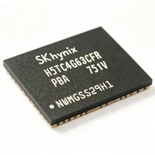
H5AN8G6NCJR-xxC - 8Gb DDR4 SDRAM 2666Mbps | SK Hynix
MPN: H5AN8G6NCJR-xxC ✓ NakahandaH5AN8G6NCJR-xxC Ulas
DDR4 SDRAM (Double Data Rate Fourth Generation Synchronous Dynamic Random Access Memory) is a type of volatile memory that transfers data on both edges of the clock signal, doubling the data rate compared to single-data-rate SDRAM. It is the industry standard for main memory in servers, desktops, laptops, and high-performance computing systems, offering higher bandwidth and lower power consumption than its predecessor DDR3. DDR4 operates at lower voltages (1.2V typical) and supports higher densities, making it essential for modern computing platforms.
Key features of the H5AN8G6NCJR-xxC include a data rate of 2666 Mbps (as indicated by the 'VKC' speed grade), a 1.2V power supply, and a x16 organization (8Gb density organized as 512M x 16). The device supports standard DDR4 features such as on-die termination (ODT), programmable read/write latencies, and burst lengths of 8 and 4 with burst chop. It is available in a 96-ball FBGA package, which is the standard for DDR4 memory components.
The H5AN8G6NCJR-xxC utilizes advanced CMOS process technology, enabling high-speed operation with low power consumption. The device includes a temperature-compensated self-refresh (TCSR) feature to reduce power in idle states, and supports a wide operating temperature range from 0°C to 95°C (TC) for standard operation. The memory is organized into 8 banks, providing efficient access patterns for high-bandwidth applications.
Typical applications include server main memory, desktop and laptop RAM modules, networking equipment, and high-performance embedded systems. The high density and bandwidth make it suitable for data-intensive workloads such as cloud computing, virtualization, and real-time analytics. The device is also used in memory modules (DIMMs/SO-DIMMs) for consumer and enterprise computing.
When designing with this component, ensure proper decoupling capacitors near the power pins and follow the PCB layout guidelines in the datasheet to minimize signal integrity issues. The device requires a stable 1.2V supply and a separate VPP supply of 2.5V for wordline boost. Refer to the SK Hynix datasheet for detailed timing parameters and AC/DC operating conditions.
Mga alternatibo na pwedeng ilagay na H5AN8G6NCJR-xxC — parehas na package, pin-to-pin na katugmang. Hindi kasama ang mga bahagi ng iba't-ibang package na nangangailangan ng pagpapaayos ng PCB.
Variante sa Seri na ito
Katulad na modelo sa serye na katugma sa pagpasok H5AN8G6NCJR-xxC (parehas na form factor at footprint) — pagkakaiba sa Package, Density, Organization, Burst Length, CAS Latency.
H5AN8G6NDJR-xxC
✅ Drop-In📋 Alternatibo na Reference (hindi sa katalogo)
H5AN8G8NCJR-xxC
✅ Drop-In📋 Alternatibo na Reference (hindi sa katalogo)
H5AN8G4NCJR-xxC
✅ Drop-InMagkontak para sa presyo
Tingnan ang Datasheet →H5AN8G6NAFR-xxC
✅ Drop-In ⚠️ Mga Talaan Hindi Naiwerikmo📋 Alternatibo na Reference (hindi sa katalogo)
MT41K256M16HA-125:E
✅ Drop-In ⚠️ Mga Talaan Hindi NaiwerikmoMagkontak para sa presyo
Tingnan ang Datasheet →K4B4G1646D-BYK00
✅ Drop-In ⚠️ Mga Talaan Hindi NaiwerikmoMagkontak para sa presyo
Tingnan ang Datasheet →H5AN8G6NCJR-xxC Mga Pinakamataas na Rating at Electrical Characteristics
| Uri ng Memory | DDR4 SDRAM |
| Density | 8 Gb |
| Organisasyon | 512M x 16 |
| Rate ng Data | 2666 Mbps (VKC speed grade) |
| Supply Voltage (VDD) | 1.2 V |
| VPP Supply | 2.5 V |
| Operating Temperature (TC) | 0°C to 95°C |
| Packhaging | 96-ball FBGA |
| Number of Banks | 8 |
| Burst Length | 8, 4 (with burst chop) |
| On-Die Termination (ODT) | Supported |
| Self-Refresh | Temperature-compensated (TCSR) |
| RoHS | Compliant |
| Lead-Free | Yes |
| Uri ng Pagpapasok | Surface Mount |
Pin Configuration ng H5AN8G6NCJR-xxC
| Pin A1 | VDD — Power supply (1.2V) |
| Pin A2 | DQ0 — Data input/output 0 |
| Pin A3 | DQ1 — Data input/output 1 |
| Pin B1 | VSS — Ground |
| Pin B2 | DQ2 — Data input/output 2 |
| Pin B3 | DQ3 — Data input/output 3 |
| Pin C1 | VDDQ — Data power supply (1.2V) |
| Pin C2 | DQS_t — Data strobe (true) |
| Pin C3 | DQS_c — Data strobe (complement) |
| Pin D1 | VSSQ — Data ground |
| Pin D2 | CK_t — Clock (true) |
| Pin D3 | CK_c — Clock (complement) |
Tipikal na mga Gamit
H5AN8G6NCJR-xxC ay nararapat para sa 6 aplikasyons: Server Main Memory, Desktop and Laptop RAM, Networking Equipment, Embedded Systems, High-Performance Computing, Consumer Electronics.
Server Main Memory
The H5AN8G6NCJR-xxC provides 8Gb density and 2666 Mbps bandwidth, making it ideal for server DIMM modules. Its high capacity supports virtualization, cloud computing, and large-scale data processing. The 1.2V operation reduces power consumption in data centers, while the 96-ball FBGA package enables high-density module designs. When used in RDIMMs or LRDIMMs, it delivers the performance needed for enterprise workloads.
Inirekomenda
Desktop and Laptop RAM
The H5AN8G6NCJR-xxC is used in SO-DIMM and UDIMM modules for consumer computing. Its 8Gb density allows 16GB modules with 16 devices, and the 2666 Mbps speed supports modern CPUs. The low 1.2V supply reduces heat generation, making it suitable for compact laptops. The x16 organization simplifies module design by reducing the number of devices needed for a 64-bit data bus.
Inirekomenda
Networking Equipment
In routers, switches, and network appliances, the H5AN8G6NCJR-xxC provides high-bandwidth memory for packet buffering and routing tables. Its 2666 Mbps data rate ensures fast processing of network traffic, while the 8Gb density supports large forwarding databases. The device's synchronous operation with both clock edges enables efficient data transfer in high-speed networking applications.
Inirekomenda
Embedded Systems
For high-performance embedded systems such as industrial PCs and edge computing devices, the H5AN8G6NCJR-xxC offers the density and bandwidth needed for real-time data processing. Its wide operating temperature range (0°C to 95°C) allows use in harsh environments. The 96-ball FBGA package is suitable for compact PCB designs, and the low power consumption is beneficial for power-constrained applications.
Inirekomenda
High-Performance Computing
The H5AN8G6NCJR-xxC is used in HPC systems where large memory capacity and high bandwidth are critical. Its 8Gb density allows building large memory pools, and the 2666 Mbps speed supports compute-intensive workloads like scientific simulations and AI training. The device's on-die termination and programmable latencies enable fine-tuning for maximum performance in multi-channel memory architectures.
Inirekomenda
Consumer Electronics
In high-end consumer devices such as gaming consoles and smart TVs, the H5AN8G6NCJR-xxC provides the memory bandwidth for smooth graphics and multitasking. Its 8Gb density supports large application footprints, and the 1.2V operation helps manage thermal budgets. The x16 organization is ideal for applications requiring a wide data bus, such as integrated graphics.
Inirekomenda
Buod ng mga Inirekomendang Produkto
Impormasyon ng Talumpati sa Engineering for H5AN8G6NCJR-xxC — ikabit, gabay sa disenyo, at impormasyon ng pagsunod sa kautusan.
Paunawang Hanapin
Ikabit sa Mga Alternatibo
| Parametro | Ito ang Producto | H5AN8G6NDJR-xxC | H5AN8G8NCJR-xxC | MT41K256M16HA-125:E |
|---|---|---|---|---|
| Package | 96-ball FBGA | 96-ball FBGA | 96-ball FBGA | 96-ball FBGA |
| Brand | SK Hynix | SK Hynix | SK Hynix | Micron Technology |
| Density | 8 Gb | 8 Gb | 8 Gb | 4 Gb |
| Organization | 512M x 16 | 512M x 16 | 1G x 8 | 256M x 16 |
| Data Rate | 2666 Mbps | 2666 Mbps | 2666 Mbps | 2400 Mbps |
| Supply Voltage (VDD) | 1.2 V | 1.2 V | 1.2 V | 1.2 V |
| Operating Temperature | 0°C to 95°C | 0°C to 95°C | 0°C to 95°C | 0°C to 95°C |
| RoHS | Compliant | Compliant | Compliant | Compliant |
Pangunahing mga Pagkakaiba
- Higher density than some alternatives (kumpara saMT41K256M16HA-125:E)
- Wider data bus (x16) (kumpara saH5AN8G8NCJR-xxC)
- Higher data rate (kumpara saMT41K256M16HA-125:E)
Talaan ng Disenyo
Ensure stable 1.2V VDD and 2.5V VPP supplies. Use low-ESR decoupling capacitors (e.g., 0.1uF and 1uF) placed close to each VDD and VDDQ pin. The VPP supply is critical for wordline boost; inadequate decoupling can cause write failures.
Follow the PCB layout guidelines in the SK Hynix datasheet for DDR4 routing. Maintain controlled impedance for DQ, DQS, and clock signals (typically 40-50 ohms single-ended). Keep trace lengths matched within +/- 10 mils for data groups to ensure signal integrity at 2666 Mbps.
The device operates up to 95°C TC. In high-density modules, ensure adequate airflow or heatsinking to keep the junction temperature within limits. The 96-ball FBGA package has a thermal resistance of approximately 20°C/W; calculate power dissipation based on operating conditions.
Impormasyon ng Pagsunod sa Kautusan
RoHS compliant per SK Hynix datasheet. AEC-Q100 not applicable for memory components.