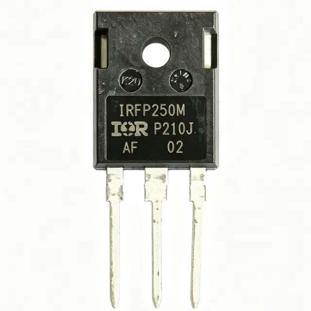
IRFP250MPBF - 200V 30A N-Channel HEXFET MOSFET | Infineon
料号: IRFP250MPBF ✓ 量产中| 数量 | 单价 | 小计 |
|---|---|---|
| 1 | $4.2 | $4.20 |
| 10 | $3.78 | $37.80 |
| 100 | $3.36 | $336.00 |
| 500 | $2.95 | $1,475.00 |
| 1,000 | $2.55 | $2,550.00 |
IRFP250MPBF 概述
A power MOSFET (Metal-Oxide-Semiconductor Field-Effect Transistor) is a voltage-controlled semiconductor switch used to switch or amplify power in electronic circuits. Within the semiconductor taxonomy, MOSFETs sit under discrete semiconductors -> transistors -> MOSFETs; the N-channel enhancement-mode variant is the most common type used in switching power supply, motor drive, and inverter applications because it offers lower on-resistance per die area than equivalent P-channel parts.
Key features include a 200V drain-to-source breakdown voltage (Vds), 30A continuous drain current (Id) at Tc=25°C, 75 mΩ maximum static on-resistance (RDS(on)) at Vgs=10V, and a power dissipation rating of 214W (Tc). The device is avalanche-rated and characterized for fast switching, making it well suited for hard-switched topologies. A typical gate threshold Vgs(th) of 4V and total gate charge of 82 nC (Qg) allow simple gate-drive compatibility with standard 10V MOSFET drivers.
Internally, the IRFP250MPBF uses Infineon's proprietary HEXFET cell geometry with a vertical DMOS structure, achieving low RDS(on) while preserving a robust body diode for inductive-load switching. The TO-247AC package provides a low thermal resistance path through the metal tab, enabling the 214W power rating at case temperatures up to 25°C and supporting high-current pulsed operation above 100A for short durations.
Typical applications include switch-mode power supplies (SMPS), DC-DC converters, motor drives, uninterruptible power supplies (UPS), solar inverters, and high-current switching circuits. The wide 200V rating also makes it suitable for offline PFC stages, full-bridge converters, and automotive 48V mild-hybrid systems where avalanche ruggedness is required.
When designing with this part, verify that the switching frequency and gate-drive circuit stay within the safe operating area (SOA) at the worst-case load. Always use a gate resistor (typically 10-100 Ω) to control dv/dt and ringing, and ensure the heatsink is sized so the junction temperature stays below 175°C under maximum steady-state dissipation.
This page synthesizes distributor pricing, drop-in alternatives, and practical design notes not found in the manufacturer datasheet.
直接替换替代料: IRFP250MPBF ——相同封装,引脚兼容。需要 PCB 改动的不同封装料号已排除。
本系列中的变体
可与以下型号直接替换的同系列型号: IRFP250MPBF (相同外形与封装尺寸) ——差异在于 Technology, Part Number, Manufacturer, Operating Temperature Range, Avalanche Rated.
快速对比工具——选择替代料号进行并排对比:
IRFP250NPBF
✓ 有现货
$1.78 / 个
查看数据手册 →STW45NM50
✓ 有现货
$9.5455 / 个
查看数据手册 →IRF3710STRLPBF
✓ 有现货
$1.23 / 个
查看数据手册 →IRFP250PBF
📋 参考替代料(不在目录中)
IRFB4710PBF
📋 参考替代料(不在目录中)
IRFP260NPBF
📋 参考替代料(不在目录中)
IRFP250MPBF 最大额定值与电气特性
| Manufacturer | Infineon Technologies (formerly International Rectifier) |
| Part Number | IRFP250MPBF |
| 晶体管类型 | N-Channel MOSFET |
| Technology | HEXFET (IR MOSFET) |
| Drain-Source Voltage (Vds) | 200 V |
| Continuous Drain Current (Id) at Tc=25C | 30 A |
| Static Drain-Source On-Resistance (RDS(on)) | 75 mOhm max @ Vgs=10V |
| Gate-Source Threshold Voltage (Vgs(th)) | 4 V (typ) |
| Total Gate Charge (Qg) | 82 nC |
| Power Dissipation (Pd) at Tc=25C | 214 W |
| 工作结温 | -55C to +175C |
| 封装 / 外壳 | TO-247AC (3-pin + tab) |
| 安装类型 | Through Hole |
| 引脚数 | 3 |
| Avalanche Rated | Yes |
| RoHS 状态 | Compliant |
| Lead-Free | Yes |
| MSL 等级 | 1 (unlimited) |
IRFP250MPBF 引脚配置
| 引脚 1 | Gate — Gate control input (drive with 10V Vgs for full RDS(on)) |
| 引脚 2 | Drain — Drain connection (also bonded to metal mounting tab) |
| 引脚 3 | Source — Source return (power and signal ground reference) |
安全工作区 (DC, Tc=25C)
典型应用
IRFP250MPBF 适用于 7 应用s: Switch-Mode Power Supplies (SMPS), DC-DC Converters (Buck/Boost), Motor Drives (H-Bridge / 3-Phase Inverter), Uninterruptible Power Supplies (UPS), Solar Micro-Inverters and Power Optimizers, Automotive 48V Mild-Hybrid Systems, Industrial Welding and Plasma Cutters.
Switch-Mode Power Supplies (SMPS)
The IRFP250MPBF serves as the main switching element in 200V-class SMPS topologies including half-bridge, full-bridge, and forward converters. With 200V Vds rating and 75 mOhm RDS(on), it handles 150V DC bus rails common in telecom and industrial supplies with adequate margin. The 82 nC total gate charge allows operation at 50-100 kHz switching frequencies with standard 10V gate drivers, while the TO-247AC package dissipates heat efficiently via the metal tab.
推荐
DC-DC Converters (Buck/Boost)
The IRFP250MPBF is well suited for high-current buck and boost DC-DC converters operating from 48V-150V input rails. Its 30A continuous drain current and 200V Vds rating provide safety margin above 150V nominal bus voltages seen in industrial and telecom systems. The fast switching speed and low gate charge (82 nC) minimize switching losses, while the TO-247AC package simplifies heatsink mounting in through-hole designs.
推荐
Motor Drives (H-Bridge / 3-Phase Inverter)
The IRFP250MPBF works as a low-side or high-side switch in brushed DC H-bridges and 3-phase inverters driving 200V-class BLDC and AC motors. Its 30A continuous current matches small to medium motor ratings (1-3 HP), and the avalanche rating provides ruggedness against the inductive kickback of motor windings. The TO-247AC package bolts directly to the chassis or motor-controller heatsink for efficient thermal management under PWM switching.
推荐
Uninterruptible Power Supplies (UPS)
The IRFP250MPBF supports UPS inverter stages converting battery DC to AC mains power. Its 200V Vds handles 192V nominal battery strings with adequate derating margin, and 30A continuous current suits 1-2 kVA single-phase inverter designs. The avalanche-rated body diode simplifies dead-time handling, while the rugged HEXFET construction supports the high di/dt transients typical in UPS load steps.
推荐
Solar Micro-Inverters and Power Optimizers
In solar micro-inverter and power-optimizer designs, the IRFP250MPBF acts as the primary switching element in the DC-DC stage converting panel voltage (up to 150V VOC for 60-cell panels) to a higher DC bus. Its 200V Vds provides safety margin above the panel open-circuit voltage under cold-condition extremes. The fast switching and low gate charge keep efficiency above 95% in 200-400W micro-inverter modules.
推荐
Automotive 48V Mild-Hybrid Systems
The IRFP250MPBF's 200V Vds rating comfortably covers 48V mild-hybrid bus rails (with full 4x derating) and provides headroom for transients on 12V/48V dual-battery vehicles. With 30A continuous current, it switches 1-1.5 kW DC-DC converter stages linking the 48V and 12V buses. The TO-247AC through-hole package supports the bolt-down thermal mounting common in automotive underhood electronics where vibration and thermal cycling are severe.
推荐
Industrial Welding and Plasma Cutters
In welding and plasma-cutting inverter designs, the IRFP250MPBF serves as the main switching transistor in the 20-50 kHz primary-side bridge. The 200V Vds supports rectified mains (170V peak for 120VAC, 340V peak for 230VAC) with appropriate derating and snubber design. The 214W power dissipation rating and TO-247AC package handle the high thermal stress of welding duty cycles where the MOSFET sees both high current and high voltage simultaneously.
推荐
推荐产品汇总
工程参考数据: IRFP250MPBF ——对比、设计指导和合规信息。
选型指南
与替代料对比
| 参数 | 本产品 | IRFP250NPBF | IRFP250PBF | IRFB4710PBF | IRFP260NPBF | STW45NM50 |
|---|---|---|---|---|---|---|
| Package | TO-247AC (through-hole) | TO-247AC - same | TO-247AC - same | TO-247AC - same | TO-247AC - same | TO-247 - same |
| Brand | Infineon | Infineon | Infineon | Infineon | Infineon | STMicroelectronics |
| Drain-Source Voltage Vds | 200 V | 200 V | 200 V | 100 V | 200 V | 500 V |
| Continuous Drain Current Id | 30 A | 30 A | 30 A | 75 A | 50 A | 45 A |
| RDS(on) max @ Vgs=10V | 75 mOhm | 45 mOhm | 75 mOhm | 14 mOhm | 40 mOhm | 120 mOhm |
| Power Dissipation Pd @ Tc=25C | 214 W | 214 W | 214 W | 300 W | 280 W | 300 W |
| RoHS Compliance | Yes (PbF suffix) | Yes | Yes | Yes | Yes | Yes |
| Avalanche Rated | Yes | Yes | Yes | Yes | Yes | Yes |
关键差异点
- Lower RDS(on) in same TO-247AC footprint (对比 IRFP250NPBF)
- Higher current headroom in same package (对比 IRFP260NPBF)
- Proven HEXFET ruggedness and avalanche rating (对比 STW45NM50)
- RoHS compliance for global market access (对比 Original IRFP250 (non-PbF))
设计说明
The TO-247AC package is rated for 214W power dissipation at Tc=25C, but this rating falls linearly to zero at Tj(max)=175C. For continuous operation at 30A, the worst-case RDS(on)*I^2 conduction loss at Tj=150C rises approximately 1.5x above the 25C datasheet value. Estimate: at 17A continuous and RDS(on)=75 mOhm, conduction loss is ~22W and requires a heatsink with thermal resistance below 5 C/W to keep Tj below 150C. Always use thermal interface material and torque the mounting screw to the datasheet specification (typically 0.7 N*m) to minimize tab-to-heatsink thermal resistance.
For through-hole TO-247AC designs, keep the source lead length short and use wide copper pours on both sides of the PCB connected to the drain tab via the mounting hole. Place the gate-drive resistor (typically 10-47 ohm) close to the gate pin to minimize parasitic inductance. Add a local 100nF-1uF ceramic bypass capacitor between the gate-driver supply and ground, located within 5mm of the IC, to suppress switching noise coupling into the gate.
Never exceed Vgs(max) of +/-20V during switching transients - gate over-voltage can punch through the thin gate oxide and destroy the device. Always include a 10V Zener diode (or TVS) between gate and source to clamp inductive transients. Also verify that the avalanche energy (EAS) rating in the datasheet is not exceeded during turn-off of inductive loads; otherwise add a freewheel diode (Schottky or fast-recovery) across the load.
Minimize the loop inductance between the drain, source, and the DC-link bypass capacitor. A high di/dt loop area creates voltage overshoot that may exceed Vds rating and trigger avalanche breakdown. Use a low-ESR DC-link film or ceramic capacitor bank placed within 20mm of the MOSFET source pins, and keep the source return path direct to minimize the gate-source loop inductance that can cause gate-oscillation or dv/dt-induced turn-on.
合规信息
PbF suffix indicates RoHS lead-free compliance per Infineon product page. Not AEC-Q100 qualified - this is a through-hole industrial part. Halogen-free status not explicitly stated in verified data.

