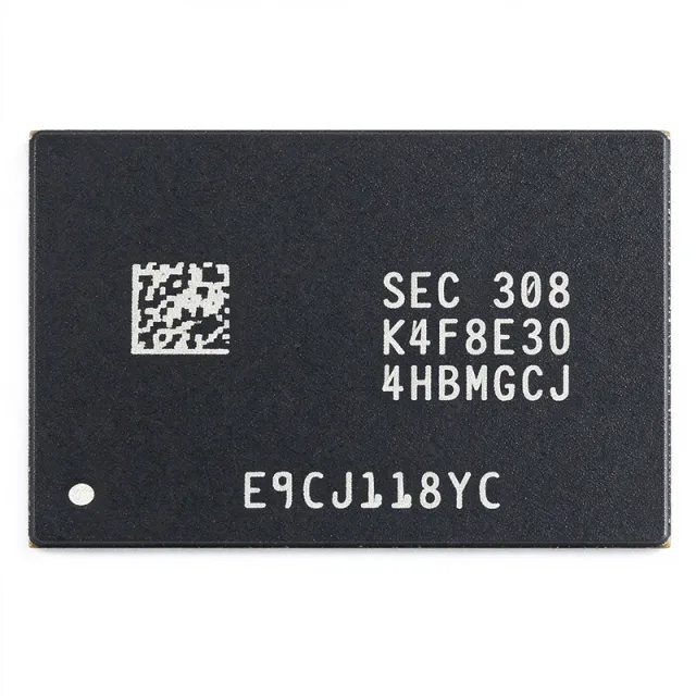
K4F8E304HB-MGCJ - 8Gb LPDDR4 x32 3733Mbps DRAM | Samsung
料号: K4F8E304HB-MGCJ ✓ 量产中| 数量 | 单价 | 小计 |
|---|---|---|
| 1 | $3.13 | $3.13 |
| 10 | $2.98 | $29.80 |
| 100 | $2.82 | $282.00 |
| 500 | $2.68 | $1,340.00 |
| 1,000 | $2.55 | $2,550.00 |
K4F8E304HB-MGCJ 概述
LPDDR4 (Low Power Double Data Rate 4) is a JEDEC-standardized synchronous DRAM designed for mobile and embedded systems, offering high bandwidth at substantially lower power than DDR3/DDR4. Within the memory hierarchy, it sits under DRAM -> SDRAM -> volatile memory and serves as the main working memory for application processors in smartphones, tablets, and embedded computing modules.
Key features include 8Gb density on a x32 data bus, a 3733 Mbps maximum data rate (1866 MHz clock), and 1.1V VDD core operation with a separate 1.8V rail per distributor data. The low voltage reduces dynamic and standby power, extending battery life in portable devices, while the wide x32 bus simplifies layout versus x16 stacking in bandwidth-limited designs.
Technically, the device is fabricated on Samsung's advanced DRAM process and complies with the JEDEC LPDDR4 standard, ensuring interoperability with mainstream mobile and embedded SoCs. It supports power-saving modes including deep power-down and self-refresh to minimize idle current, and operates across -25C to +85C per distributor listings, suiting industrial as well as consumer environments.
Typical applications include smartphones and tablets, AI accelerators and edge inference, VR headsets, wearables, industrial controllers, and computing modules where firmware boot, embedded logging, and high-bandwidth working memory are required.
Design consideration: follow controlled-impedance, length-matched routing for the 3733 Mbps interface and place decoupling capacitors close to each VDD ball group; adequate power integrity is essential at full data rate.
This page synthesizes distributor pricing, drop-in alternative cross-references, and practical design guidance not found in the manufacturer datasheet.
直接替换替代料: K4F8E304HB-MGCJ ——相同封装,引脚兼容。需要 PCB 改动的不同封装料号已排除。
快速对比工具——选择替代料号进行并排对比:
K4F8E304HB-MGCL
📋 参考替代料(不在目录中)
AS4C256M32MD4-062BAN
📋 参考替代料(不在目录中)
K4F8E304HB-MGCJ 最大额定值与电气特性
| 存储器类型 | LPDDR4 SDRAM (Mobile DRAM) |
| Density | 8 Gbit |
| 存储组织 | 256M x32 |
| 数据速率 | 3733 Mbps |
| Clock Frequency | 1866 MHz |
| Core Supply Voltage (VDD) | 1.1 V |
| Interface Supply Voltage (VDDQ) | 1.1 V |
| I/O Supply (VDD2) | 1.8 V |
| 接口类型 | Parallel (LPDDR4) |
| 工作温度 | -25C to +85C |
| 封装 | 200-ball FBGA (TFBGA-200) |
| 安装类型 | Surface Mount |
| Power-Saving Modes | Deep power-down, self-refresh |
| Standard Compliance | JEDEC LPDDR4 |
| RoHS 状态 | Compliant |
| Typical Applications | Mobile, AI, VR, wearables, industrial controllers |
K4F8E304HB-MGCJ 200-ball fbga (tfbga-200) 引脚配置指南
K4F8E304HB-MGCJ(200-ball fbga (tfbga-200) 封装)的引脚配置。 该数字 IC 包含 GPIO、通信接口(UART、SPI、I2C)和电源引脚。请参阅制造商数据手册以了解复用引脚功能和配置选项。对嵌入式系统设计和 PCB 布局至关重要。

暂无详细引脚数据: K4F8E304HB-MGCJ.
请参阅 数据手册 以查看完整引脚配置。
典型应用
K4F8E304HB-MGCJ 适用于 6 应用s: Smartphones and Tablets, Edge AI and AI Accelerators, VR Headsets and Wearables, Industrial Controllers and Computing Modules, Embedded Logging and Firmware Boot Systems, High-Resolution Display and Graphics Systems.
Smartphones and Tablets
The K4F8E304HB-MGCJ was designed for exactly this class of device: its 8Gb density in a single x32 FBGA-200 die lets flagship and mid-range phones reach 2-4 GB RAM with only one or two packages, saving board area versus stacked DDR3. Its 3733 Mbps data rate delivers over 14.9 GB/s of peak bandwidth per package, enough for 4K video decode and heavy multitasking, while 1.1V VDD/VDDQ operation cuts memory-subsystem power - typically the largest consumer after the SoC. Deep power-down and self-refresh modes keep standby current minimal when the screen is off. Place the DRAM within the processor's specified length-matched zone and follow the SoC vendor's fly-by routing rules to close timing at full speed.
推荐
Edge AI and AI Accelerators
Edge AI inference is memory-bandwidth-bound: neural network weights and activation maps stream continuously from DRAM, so the K4F8E304HB-MGCJ's 3733 Mbps x32 interface (over 14.9 GB/s per package) directly raises inference throughput versus 2133-class LPDDR4. Samsung's own positioning explicitly targets AI workloads in ultra-thin devices. The 8Gb single-die density suits vision and audio models in the 100 MB to 1 GB parameter range, and 1.1V operation helps meet the thermal budgets of fanless edge nodes. Use multiple packages on independent chip-selects if the memory controller supports channel interleaving, which hides refresh latency and sustains real-time frame processing in camera-based inspection or robotics platforms.
推荐
VR Headsets and Wearables
VR headsets demand two high-resolution, low-latency display pipelines plus sensor fusion, making bandwidth the limiting resource; the K4F8E304HB-MGCJ's 3733 Mbps rate sustains 90+ Hz frame updates for dual panels. Samsung specifically cites VR and wearables as target markets for its LPDDR4 line. The 200-ball FBGA package and 1.1V rail fit the tight thermal and space envelopes of head-mounted and wrist-worn products, where every 100 mV of rail reduction reduces both DRAM heat and battery drain. Because these devices run in continuous self-refresh between render bursts, verify idle current in your power budget and ensure the PMIC sequencer respects LPDDR4 power-up ordering (VDD before VDDQ) to avoid latch-up during battery-powered cold boot.
推荐
Industrial Controllers and Computing Modules
Industrial controllers and COM Express/SOM compute modules use LPDDR4 for deterministic, power-efficient working memory; the K4F8E304HB-MGCJ's -25C to +85C rating covers most factory-floor environments per distributor data, and Samsung's product overview names industrial controllers and computing modules among its intended uses. The 8Gb x32 organization supports firmware boot, embedded logging, and real-time control loops with headroom for protocol stacks and local data buffering. Its JEDEC LPDDR4 compliance ensures interoperability with industrial SoCs from multiple vendors. For long-lifecycle industrial BOMs, qualify a second source such as the Alliance AS4C256M32MD4-062BAN early, and confirm supplier date-code and traceability policies - commodity DRAM sourcing risk, not electrical performance, is the main industrial concern.
推荐
Embedded Logging and Firmware Boot Systems
Systems that log data continuously - gateways, recorders, telemetry nodes - benefit from the K4F8E304HB-MGCJ as a fast volatile buffer that absorbs burst data before it is committed to slower non-volatile storage. Samsung's overview lists embedded logging and firmware boot among this part's roles. The 8Gb capacity provides several minutes of buffered high-rate data, while the 3733 Mbps x32 bus prevents the memory from throttling acquisition front ends. Use LPDDR4 self-refresh to retain logged buffers through brief power events, and design brown-out handling so the SoC flushes DRAM-resident logs to flash before rail collapse. Verify your bootloader initializes DRAM with the correct timing registers for the MGCJ speed bin to avoid intermittent cold-boot failures.
推荐
High-Resolution Display and Graphics Systems
Frame buffers for high-resolution displays consume bandwidth linearly with pixel rate: a 4K60 panel alone requires several GB/s just for refresh, before compositing overhead. The K4F8E304HB-MGCJ's 3733 Mbps x32 interface provides the headroom graphics and display SoCs need, and its 8Gb density accommodates triple-buffering at 4K resolutions. Samsung markets its LPDDR4 family for high-resolution display applications in thin devices. In display-heavy designs, configure the memory controller's QoS arbitration so display fetches preempt CPU traffic, and keep the DRAM physically close to the SoC - short, impedance-controlled routing preserves eye margins at 1866 MHz and reduces EMI from the high-speed DQ/CA bus.
推荐
推荐产品汇总
工程参考数据: K4F8E304HB-MGCJ ——对比、设计指导和合规信息。
选型指南
与替代料对比
| 参数 | 本产品 | K4F8E304HB-MGCL | AS4C256M32MD4-062BAN |
|---|---|---|---|
| Package | 200-ball FBGA (TFBGA-200) | 200-ball FBGA (TFBGA-200) - same | 200-ball FBGA (TFBGA-200) |
| Brand | Samsung Electronics | Samsung Electronics | Alliance Memory |
| Density | 8 Gbit | 8 Gbit | 8 Gbit |
| Organization | 256M x32 | 256M x32 | 256M x32 |
| Data Rate | 3733 Mbps | 3733 Mbps | 3733 Mbps |
| Supply Voltage | 1.1 V (VDD/VDDQ), 1.8 V (VDD2) | 1.1 V / 1.8 V | 1.1 V / 1.8 V |
| JEDEC LPDDR4 Compliance | Yes | Yes | Yes (per Alliance comparison doc) |
关键差异点
- Highest LPDDR4 speed bin in the K4F8E304HB family (对比 K4F8E304HB-MGCL)
- Documented second-source ecosystem (对比 AS4C256M32MD4-062BAN)
- x32 bus width in a single 8Gb die (对比 AS4C256M32MD4-062BAN)
设计说明
At 3733 Mbps, LPDDR4 DQ and CA nets carry sub-300 ps unit intervals. Follow the SoC vendor's LPDDR4 routing guide: 40-ohm single-ended / 80-ohm differential controlled impedance, length matching within the controller-specified skew window (typically a few mils per inch of trace), and solid, unbroken reference planes under the entire bus. Keep the DRAM within the SoC's specified keep-in zone - typically under 40 mm of routing - and avoid stubs on DQS/CK differential pairs. Simulate the fly-by clock topology with IBIS models before tape-out.
The K4F8E304HB-MGCJ requires a 1.1V VDD/VDDQ rail and a 1.8V interface rail per distributor data. At full bandwidth, peak current transients are sharp (hundreds of mA in nanoseconds), so combine bulk capacitance (22-47 uF) with dense 0.1 uF/0.01 uF decoupling at each ball group. Use a PMIC with LPDDR4-specific rails and respect the power-up sequence (VDD before/at VDDQ) and power-down ordering to avoid latch-up. Verify deep power-down and self-refresh entry/exit timing against the datasheet to meet your idle-power budget.
LPDDR4 controllers require per-bin training: if you swap the Samsung K4F8E304HB-MGCJ for a second source such as the Alliance AS4C256M32MD4-062BAN, re-run memory training and read/write margining on the new part, and update MR (mode register) settings and drive-strength/ZQ calibration if the vendor defaults differ. Do not assume same-density means identical - confirm the JEDEC ball map on your footprint, and always validate at temperature extremes, since margins that pass at room temperature can fail at -25C or +85C.
Estimated: DRAM power at 3733 Mbps typically falls in the 300-600 mW range for 8Gb x32 under mixed read/write activity (input estimate: activity mix 50/50, 1.1V rail). The 200-ball FBGA dissipates this through the PCB, so provide thermal vias under the package tied to inner ground planes. In sealed industrial enclosures, keep PCB copper area under the DRAM generous and verify junction temperature stays below the datasheet maximum at the +85C ambient rating upper limit.
合规信息
RoHS compliant per JLCPCB and distributor listings. REACH, halogen-free, and conflict-minerals status not stated in provided data - request declarations from Samsung Semiconductor.



