FPGA & CPLD
Products (6357)

EP20K200CQ208C8 - APEX 20KC FPGA 200K Gates | Altera
The Altera (now Intel) EP20K200CQ208C8 is a member of the APEX 20KC programmable logic family, providing 200,000 system gates, 8,320 logic elements, and 106,496 bits of embedded RAM in a 208-pin QFP (PQFP-208, 28x28 mm) package. Fabricated on a 0.18 µm (0.15 µm effective) CMOS process, the device operates from a 1.71 V to 1.89 V core supply (1.8 V nominal) and supports a maximum internal clock frequency of approximately 301 MHz. The 'C8' speed grade places the part in the commercial-temperature category, while the 'CQ' package code designates the 208-pin plastic QFP with gull-wing leads. A Field Programmable Gate Array (FPGA) is a type of programmable logic device (PLD) that allows hardware designers to configure logic blocks, routing, and I/O after manufacture. FPGAs sit within the broader hierarchy of programmable logic (PLD > CPLD > FPGA > system-on-chip FPGA), occupying the high-density, high-performance segment used for glue logic, DSP pipelines, bus interfaces, and prototype ASIC replacement. The APEX 20KC family specifically combines look-up-table (LUT) based logic with embedded MultiCore memory blocks, distinguishing it from earlier CPLD-style architectures. Key features of the EP20K200CQ208C8 include 8,320 logic elements, 106,496 bits of embedded SRAM (typically organized as ESBs - Embedded System Blocks), LVTTL and LVCMOS I/O support, in-system programmability via JTAG, and 144 user-I/O pins maximum. The 208-pin PQFP provides through-hole-compatible gull-wing leads suitable for sockets and rework-friendly assembly, and the device supports Altera's Quartus design flow for synthesis, place-and-route, and timing analysis. In terms of architecture depth, the APEX 20KC combines four-input LUTs with embedded memory blocks and dedicated high-speed paths between MegaLAB columns, enabling efficient implementation of datapath-heavy designs. The 1.8 V core, while low for its era, demanded multiple supply rails on the board; modern designs have since shifted to 2.5 V, 3.3 V, and sub-1 V FPGAs. Typical applications include legacy telecom interface cards, industrial control backplanes, and prototype ASIC replacement in mid-density glue-logic and DSP pre-processing roles. The QFP-208 package also makes it useful where socketed or hand-replaceable logic is required for field serviceability. A common modern use is sustaining production of end-of-life equipment where the original part must be sourced through distribution or licensed remanufacturing. Designers should note that the APEX 20KC family is now classified as NRND/EOL by Intel (which acquired Altera in 2015). Supply is typically through authorized distributors, franchised brokers, or authorized remanufacturers; verify RoHS and original-component traceability when sourcing from the secondary market. This page consolidates distributor pricing, drop-in alternative listings, and practical design guidance for engineers maintaining legacy systems based on the EP20K200CQ208C8.
EP20K200CQ208C8ES - APEX 20KC FPGA 200K Gates 208-BFQFP
The Altera (Intel® Programmable Solutions Group) EP20K200CQ208C8ES is an APEX 20KC family Field Programmable Gate Array (FPGA) delivering 200K system gates with 8320 logic elements in a 208-pin BFQFP (PQFP) plastic quad flat pack package. It provides 136 user I/Os and a maximum internal clock frequency of 301.21 MHz, fabricated on a 0.15 µm CMOS process with a 1.8 V core supply (VCCINT range 1.71 V to 1.89 V). An FPGA (Field Programmable Gate Array) is a semiconductor device containing programmable logic blocks, configurable interconnect, and I/O cells that engineers can reconfigure after manufacturing to implement custom digital circuits. FPGAs sit within the broader hierarchy: programmable logic -> logic IC -> integrated circuit -> semiconductor. APEX 20KC extends Altera's APEX 20K MultiCore architecture with CAM (Content Addressable Memory) support and LVDS-capable high-speed I/O. Key features include 106,496 RAM bits of embedded system memory distributed across ESBs (Embedded System Blocks), 4 phase-locked loops (PLLs) for clock management, MultiVolt I/O supporting 1.8 V/2.5 V/3.3 V interfaces, and JTAG-based IEEE 1149.1 boundary-scan testing. The device supports hot-socketing insertion and in-system programmability via Altera's serial configuration (EPC16, EPC8) or JTAG chains. The APEX 20KC architecture combines four types of building blocks - LUTs for logic, ESBs for memory/PLL, FastTrack interconnect, and MegaLAB structures - enabling designs that mix datapath, control, and memory. The 200K-gate capacity positioned this family as a mid-density workhorse for telecom, networking, and DSP-intensive applications in the early 2000s. Typical applications include telecommunications line cards, network switches and routers, DSP co-processing, industrial control systems, and military/aerospace prototyping. The BFQFP-208 footprint was widely supported by JTAG programmers and Altera's ByteBlaster/USB-Blaster download cables. When designing, account for the BFQFP-208 thermal envelope (typical θJA ≈ 30 °C/W) and provide adequate decoupling (100 µF bulk + 0.1 µF ceramic per supply pin group). Configuration must complete within the device's POR (power-on reset) window; ensure VCCINT reaches 1.71 V before MSEL pin states are sampled. This page synthesizes distributor stock levels, parameter cross-references, and design guidance not consolidated in the original datasheet, enabling faster design-in for both new designs and legacy board replacements.

EP20K200CQ208C8N - APEX 20KC FPGA 1.8V | Altera
The Altera EP20K200CQ208C8N is an APEX 20KC field-programmable gate array (FPGA) with 8320 logic elements, 106,496 RAM bits, and 144 user I/O pins, housed in a 208-pin PQFP/BFQFP package. It is manufactured in a 0.15 um process with a 1.8 V core supply and is listed with a 301.21 MHz maximum internal frequency. A field-programmable gate array is an integrated circuit whose digital logic can be configured after manufacturing to implement arbitrary functions, ranging from simple glue logic to complete digital subsystems. FPGAs form the programmable logic class of semiconductors, standing between standard-cell ASICs and software-programmable processors. This EP20K200 variant belongs to the Altera APEX 20KC family, which targets high-density gate-array replacement and memory-rich protocol processing. Understanding this hierarchy helps engineers decide when an FPGA is needed: design changes can be handled in software/AHDL/Verilog rather than by silicon respin. Key features of the EP20K200CQ208C8N include 8320 logic elements, 200K typical gates, 144 user I/O pins, and 106,496 bits of embedded RAM. The 208-pin PQFP package uses gull-wing leads and is suited to moderate pin-count boards without BGA assembly cost. The device also has four dedicated inputs and is described as a loadable PLD, meaning it can be configured in-system. The N suffix is used by Altera to indicate the Pb-free/RoHS-compliant ordering option in many APEX part numbers. The APEX 20KC architecture combines logic elements and memory blocks on a single die, enabling FIFOs, ATM cells, and packet buffers to be implemented without external SRAM. At 301.21 MHz maximum internal frequency and with a 1.8 V core, this device offers a practical balance of performance and power for mid-density FPGA applications. The 0.15 um process technology is a key enabler of this density in a surface-mount QFP package. Typical applications include telecom line-card control logic, industrial automation interfaces, medical image capture and control chains, video and display controllers, and test-and-measurement waveform engines. The 106,496 RAM bits support distributed buffering and small FIFOs, while the 144 I/O pins can connect to parallel ADCs/DACs, SRAM, and backplane buses. When designing the EP20K200CQ208C8N into a PCB, pay close attention to the 1.8 V core supply and its decoupling, and verify the configuration source before power-on. The APEX 20K family datasheet should be consulted for power sequencing, I/O bank setup, and thermal-package mechanical information. This page synthesizes distributor availability, drop-in CQ208 alternatives, comparison data, and practical design notes not provided in the summary search snippets, making it a useful starting point for engineers assessing the EP20K200CQ208C8N in legacy or new designs.
EP20K200CQ208C9 - APEX-20KC FPGA 200K Gates | Intel
The Intel EP20K200CQ208C9 is a 1.8V APEX-20KC programmable logic device offering 200K typical gates, 8,320 logic elements/cells, up to 250 MHz internal operation, and 106,496 total RAM bits in a 208-pin PQFP/BFQFP (28x28 mm) package. An FPGA (field-programmable gate array) is a semiconductor device containing programmable logic blocks, embedded memory, and configurable interconnect that can be programmed after manufacturing to implement custom digital logic. The EP20K200CQ208C9 belongs to the APEX-20KC family, which sits within the broad programmable logic hierarchy that includes CPLDs, FPGAs, and system-level integration devices used for board-level digital functions. Key features from the verified web data include a 0.15um process technology, a core supply voltage range of 1.71V to 1.89V, 106,496 total RAM bits, and 8,320 logic cells. The 208-pin PQFP/BFQFP package provides a large pin count for I/O-intensive designs, while the 250 MHz family rating allows fast state machines, datapath processing, and bus-interface logic. The C9 suffix indicates the specific ordering and speed-grade option, and the device is described as a CMOS loadable PLD with roughly 2 ns internal signal delay. Architecturally, APEX-20KC devices are SRAM-based FPGAs. They combine look-up-table logic with embedded RAM and high-speed routing resources, enabling designers to implement FIFOs, protocol controllers, and custom logic without many external glue parts. Because they are SRAM-based, EP20K200CQ208C9 devices need a configuration bitstream loaded after every power-up, normally via an Altera configuration device or download cable, before the I/O pins become active. Typical application fields include telecom line cards, network routers, industrial digital control, and test instrumentation, where the medium-density logic cells, 106,496 bits of embedded RAM, and 1.8V core help balance performance and power. The device is well suited to replace multiple discrete logic devices on a single board, reducing part count and easing board revision. Design consideration: verify that your configuration source can handle a 1.8V APEX-20KC device in the 208-pin PQFP package, and place adequate decoupling capacitors across the power and ground pins because the core can switch large transient currents. Signal integrity of the PQFP leads is also a board-layout concern at high output drive settings. This page synthesizes distributor stock references, market pricing, pin-compatible family alternatives, and practical design notes that go beyond the raw information found in the manufacturer datasheet.

EP20K200CQ240C7 - 8320 LE APEX-20KC FPGA | Altera
The Altera EP20K200CQ240C7 is an APEX-20KC Field-Programmable Gate Array (FPGA) with 8,320 logic elements, 106,496 RAM bits, and 168 user I/Os, housed in a 240-pin BFQFP package. Distributor listings describe the device as IC FPGA 168 I/O 240QFP, confirming its role as a high-I/O logic device for board-level reconfigurable designs requiring embedded memory and programmable logic. An FPGA is an integrated circuit containing programmable logic blocks and programmable interconnect. An engineer configures the device after manufacturing using a hardware description language such as VHDL or Verilog. Unlike a fixed ASIC, the EP20K200CQ240C7 can implement different functions during development or at run time when paired with configuration memory. In a signal-chain hierarchy, an FPGA often sits between data converters and processors, handling parallel data movement, protocol timing, and custom DSP arithmetic. The main verified specifications are 8,320 logic elements, giving a 200K-class APEX-20K density level; 106,496 RAM bits for FIFOs, packet buffers, and dual-port memory functions; and 168 user I/Os for wide parallel buses and external control. The device is supplied in a 240-pin BFQFP, a surface-mount plastic quad flat pack footprint used by many legacy industrial and communication boards. Distributor data consistently identifies the part as an APEX-20KC product, with the CQ240C7 suffix indicating the package and Altera-grade ordering code. The device is now often obtained through specialty aftermarket channels, and engineers should verify current lifecycle and configuration compatibility before new designs or repair programs. Typical applications include networking protocol bridging, telecom baseband interfaces, industrial control I/O logic, test-and-measurement pattern generation, and legacy system lifecycle extension. The FPGA is especially useful where 168 I/Os must connect to ADCs, DACs, memory buses, and processors in parallel rather than through high-speed serial links. When designing with a legacy FPGA, confirm exact core and I/O supply voltages, pin numbering, and configuration scheme from the APEX-20K family datasheet before PCB layout. Since the part has been in service for many years, verify lead-free finish requirements because non-N suffix devices may not be RoHS-compliant. This page synthesizes distributor pricing, drop-in same-family alternatives, and practical design notes not found in the manufacturer datasheet, helping engineers evaluate the EP20K200CQ240C7 for both legacy and repair applications.
EP20K200CQ240C7ES - APEX 20KC FPGA 200K Gates | Intel
The Altera (now Intel) EP20K200CQ240C7ES is an APEX 20KC family field-programmable gate array (FPGA) delivering 200K system gates, 8,320 logic elements, and 106,496 RAM bits with 168 user I/Os in a 240-pin PQFP (BFQFP) package operating from a 1.8 V core supply. This device is fabricated in 0.15 um CMOS technology and is represented in distributor data with a 375.94 MHz maximum internal frequency. The ES suffix identifies an engineering sample, so designers should treat it as an early validation part rather than a production-qualified unit. An FPGA is a reconfigurable integrated circuit whose logic fabric, routing, and I/O behavior are defined after manufacturing by a configuration bitstream. The field-programmable gate array category sits above programmable logic devices in the digital logic hierarchy and includes APEX 20KC as a 1.8 V SRAM-based device architecture. Designers use FPGAs when they need hardware parallelism, mid-volume flexibility, or protocol agility that fixed ASICs or microcontrollers cannot easily provide. Key features include 200K system gates, 8,320 logic elements, 106,496 RAM bits, and 168 user I/Os. The 240-pin PQFP package provides a practical balance between routing capability and board-level manufacturability at 0.5 mm-style quad flat pack density. The 1.8 V core supply and 0.15 um CMOS process reduce dynamic power compared with older 2.5 V or 3.3 V programmable logic families while retaining a large I/O count for parallel applications. The APEX 20KC architecture combines a programmable logic core with embedded RAM and high-speed interconnect. The 8,320 logic elements can implement state machines, datapaths, and parallel processing functions, while the 106,496 RAM bits support FIFOs, small packet buffers, and lookup tables without external memory. The 168 I/Os are important for buses such as 32-bit parallel interfaces, telecommunication backplanes, or video pixel buses. The device is configured over JTAG or through an Altera configuration device such as EPC16 or EPC2. Typical applications include telecom line-card bridging, industrial control and PLC I/O processing, video/image capture preprocessing, medical instrumentation, ASIC prototyping, and interface adaptation. The engineering-sample suffix makes the part suitable for lab bring-up and prototype validation; a production-grade equivalent is normally preferred for volume systems. A key design consideration is that the FPGA is volatile and must be configured after each power-up. For the EP20K200CQ240C7ES, use a stable 1.8 V core supply and provide adequate decoupling. Take care to verify power-up sequencing and configuration source before relying on the device at system reset. This page synthesizes distributor pricing, APEX 20KC family alternatives, design notes, and datasheet locations that are not all present in a single manufacturer marketing page, giving engineers a more complete starting point for selection and procurement.
EP20K200CQ240C7N - Altera APEX 20KC FPGA | 8320 LE
The Altera EP20K200CQ240C7N is an APEX-20KC field-programmable gate array (FPGA) supplied in a 240-pin BFQFP/PQFP package. It contains 8,320 logic elements, 106,496 RAM bits, 168 user I/O pins and 4 dedicated input pins. The device operates with a nominal 1.8 V core supply, supports a 1.71 V to 1.89 V range, and is built on a 0.15 um process. According to the Microchip USA listing, its maximum clock frequency is 357.16 MHz. An FPGA is an integrated circuit whose digital logic fabric can be configured after manufacturing, allowing designers to implement custom processors, interfaces, DSP chains, and control logic without the non-recurring engineering costs of an ASIC. In the semiconductor taxonomy, an FPGA is a programmable logic device family that sits above CPLDs in logic capacity, while still being configurable in-system for rapid iteration and field updates. The EP20K200CQ240C7N differentiates itself with 8320 logic elements and 106,496 RAM bits, giving it enough fabric for moderate digital designs. The 168 user I/O lines and 4 dedicated inputs support parallel interfaces, memory buses, and communication protocols in a compact surface-mount 240-lead gull-wing package. The 1.8 V core supply reduces power consumption versus older 5 V and 3.3 V programmable devices. The part belongs to Altera's APEX 20KC family, which implemented SRAM-based programmable logic in a 0.15 um process. This provides embedded memory blocks alongside the logic array, making it suitable for designs that need on-chip buffering, FIFOs, or register files. The N suffix denotes a lead-free terminal finish, distinguishing it from the original SnPb-finished EP20K200CQ240C7. Typical applications include telecom line-card interface boards, industrial control systems, DSP front-end processing, ASIC prototyping, and communications infrastructure where moderate-density FPGA logic and many parallel I/Os are required. The 168 I/O count is sufficient for external SRAM, SDRAM, or general-purpose backplane interfaces. When designing with the EP20K200CQ240C7N, keep the 1.8 V core rail tightly regulated and provide appropriate decoupling near all supply pins. Also verify configuration compatibility with your chosen Altera configuration flow because APEX 20K devices are SRAM-based and require external configuration on power-up. This page synthesizes distributor listings, drop-in alternatives, and practical design guidance from the verified web data, adding engineering context that complements the raw datasheet specifications.
EP20K200CQ240C8ES - 200K APEX 20KC FPGA, 240-PQFP | Altera (Intel PSG)
The Altera (Intel Programmable Solutions Group) EP20K200CQ240C8ES is a member of the APEX 20KC family of Field-Programmable Gate Arrays, integrating 200K typical gates, 8,320 logic elements (cells), and 106,496 bits of embedded RAM in a 240-pin Plastic Quad Flat Pack (PQFP/BFQFP) package. It operates from a 1.8 V core supply, is built on a 0.15 µm CMOS process, and is rated for a maximum internal clock frequency of 301.21 MHz. An FPGA (Field-Programmable Gate Array) is a semiconductor device built around a matrix of configurable logic blocks (CLBs), programmable interconnects, and I/O cells, allowing the hardware functionality to be redefined after manufacturing. The APEX 20KC family sits inside Intel PSG's broader programmable-logic hierarchy: FPGA → SRAM-based LUT architecture → APEX 20K series → high-density, multi-standard I/O device class. APEX 20KC devices combine Look-Up Table (LUT)-based logic with embedded dual-port RAM and True-LVDS capable I/O, supporting system-level integration of glue logic, datapath, and high-speed I/O in a single chip. Key features of this member include 168 user I/O pins, 8320 logic elements, 106,496 bits of embedded memory, four Phase-Locked Loops (PLLs) for clock management, and support for LVDS, LVTTL, LVPECL, PCI, HSTL and SSTL I/O standards. The 'C8' speed grade and 'ES' engineering-sample suffix indicate a commercial-temperature device in a faster-than-baseline timing bin supplied as an engineering sample. Architecturally, the EP20K200CQ240C8ES uses Altera's MultiCore architecture, partitioning logic into MegaLAB structures that each contain 16 Logic Array Blocks (LABs) of 10 Logic Elements (LEs) each, sharing a single dual-port RAM block. The four embedded PLLs provide clock multiplication, phase shifting, and skew management for high-speed synchronous designs. Typical applications include telecommunications infrastructure (ATM switches, SONET/SDH framers), high-speed data acquisition and DSP coprocessor cards, industrial imaging and machine vision pipelines, network routers and switches, and military/aerospace prototyping where mid-density SRAM-based FPGA logic is required. When designing with this part, plan I/O assignment early because the 240-pin PQFP has a constrained breakout for memory buses; use the Quartus II (or legacy MAX+PLUS II) toolchain and verify pinout against the APEX 20KC datasheet before layout. This page synthesizes distributor inventory, same-family drop-in alternatives, and practical design notes beyond what the manufacturer datasheet alone provides.
EP20K200CQ240C8N - APEX 20KC FPGA 200K Gates | Altera
The Altera EP20K200CQ240C8N is an APEX 20KC programmable logic device and field-programmable gate array (FPGA) offering 200K typical gates, 8,320 logic elements, 168 dedicated I/O lines, 164 input terminals, 160 dedicated I/O pins, and a maximum internal clock frequency of 301.21 MHz. It is built with 0.15 um process technology, powered from a 1.8 V core supply, and supplied in a 240-lead PQFP (CQ240) surface-mount package. An FPGA is an integrated circuit whose logic fabric and routing are configured after manufacturing to implement arbitrary digital logic. EP20K200CQ240C8N sits in the programmable logic hierarchy: FPGA -> programmable logic device -> logic IC -> integrated circuit. This older APEX 20KC family was designed for system-level integration without the high cost of custom ASICs. On a board, it replaces discrete glue logic, microprocessor peripherals, memory controllers, and bus-bridge circuits, while retaining in-system reprogrammability through a configuration device. Key features include the large 200K-gate capacity, 8,320 logic elements for medium-density designs, 168 bidirectional I/O lines for wide parallel buses, and a rated 301.21 MHz maximum internal clock frequency. The 1.8 V core reduces dynamic power compared with earlier 2.5 V/3.3 V FPGA families, while the 0.15 um geometry provides a practical balance between density and speed. The 240-pin PQFP package is a board-friendly, conventional surface-mount format for 2000-era equipment and remains available through the legacy/surplus channel. Architecturally, the APEX 20KC family implements programmable logic with an embedded array for memory and high-speed I/O in a single device. The EP20K200 datasheet states that an Altera enhanced configuration device—a single-device, high-speed, advanced configuration solution for high-density FPGAs—contains a configuration controller and flash memory. This architecture allows the FPGA to be loaded from industry-standard configuration devices and, where necessary, re-loaded during board bring-up. The commercial C-grade and 8 speed grade balance cost and performance for communication and industrial boards. Typical applications include protocol bridging, communication line-card logic integration, DSP pre/post processing, video-image pipelines, industrial automation I/O control, and legacy FPGA replacement. The 168 I/O lines provide sufficient connectivity for 32-bit processor buses, SRAM/SDRAM interfaces, and multiple serial ports. The 301.21 MHz internal frequency supports demanding data-path applications while the 1.8 V core maintains moderate power dissipation in 240-pin boards. When designing with EP20K200CQ240C8N, provide clean, low-impedance decoupling on all 1.8 V core pins, place a suitable configuration device near the FPGA, and confirm every VCCIO bank voltage against the I/O standard used. Because this is an older device, thermal and power calculations should be checked with an early prototype before committing to the final layout. This page synthesizes distributor specifications, same-package drop-in alternatives, price tiers, and practical design notes not included in the single datasheet PDF, helping engineers select and validate this legacy FPGA faster.
EP20K200EBC356-1 - APEX 20K 200K Gates FPGA, BGA-356 | Altera
The Altera (now Intel) EP20K200EBC356-1 is a member of the APEX 20K programmable logic device (PLD) family, delivering 200,000 system gates with 8,320 logic elements in a 356-ball BGA package. The device operates from a 1.8 V core supply (range 1.71 V to 1.89 V) and is fabricated on a 0.22 µm CMOS process, targeting high-performance data-path, DSP, and register-intensive designs at up to 367 MHz internal performance. An FPGA (Field Programmable Gate Array) is a reprogrammable semiconductor that lets engineers implement arbitrary digital logic by configuring an array of configurable logic blocks (CLBs) and programmable interconnect. The APEX 20K family further distinguishes itself with MultiCore architecture, which integrates look-up-table (LUT)-based logic, product-term-based logic, and an embedded memory structure (ESB) on a single die. This multi-paradigm approach is designed for system-on-a-programmable-chip (SOPC) integration. Key features of the EP20K200EBC356-1 include 277 user I/Os, a 2.5 ns propagation delay, and the APEX 20KE enhanced-memory variant with on-chip SRAM-based memory blocks. The device is supported by the Altera Quartus II development system, providing HDL and schematic entry, synthesis, full timing simulation, SignalTap logic analysis, and device configuration. Operating temperature range is 0 °C to 85 °C (commercial grade). The MultiCore architecture makes the EP20K200EBC356-1 particularly well suited for designs that mix wide datapath logic, control-state product-term logic, and on-chip buffering. Designers can instantiate embedded memory blocks for FIFOs, dual-port RAM, or content-addressable memory without sacrificing logic resources, while LUT-based elements accelerate arithmetic, DSP, and register pipelines. Typical applications include high-speed telecommunications backplanes, ASIC prototyping, video and image processing pipelines, industrial control systems, and military/aerospace prototyping platforms. The 356-ball BGA package supports the large I/O count required for parallel memory buses, LVDS links, and processor-to-FPGA glue logic on complex boards. When designing with the EP20K200EBC356-1, ensure proper power sequencing on the 1.8 V core rail and use the Quartus II design software with the correct device pinout file for the BGA-356 package. Decoupling must follow Altera's APEX 20K reference design guidelines, and JTAG configuration via ByteBlaster or MasterBlaster is recommended for production programming. This page synthesizes distributor pricing, drop-in same-package alternatives, and practical design notes not found in the manufacturer datasheet alone, including sourcing context for legacy inventory.

EP20K200EBC356-1N - APEX 20KE 200K Gates 8320 Cells FPGA BGA-356
The Intel (formerly Altera) EP20K200EBC356-1N is a member of the APEX 20KE programmable logic device family that delivers 200,000 system gates integrating 8,320 logic elements (cells) with MultiCore architecture combining look-up table (LUT) logic and embedded memory in a single die, housed in a 356-ball BGA (EBC356, 35x35 mm LBGA) package. An FPGA (Field-Programmable Gate Array) is a semiconductor device built around an array of configurable logic blocks (CLBs), programmable interconnects, and I/O cells, allowing engineers to implement arbitrary digital logic that is re-programmable in-circuit. FPGAs sit hierarchically above ASICs in design flexibility and below microcontrollers in per-unit cost for low-volume production, and are commonly used as system-on-a-programmable-chip (SOPC) integration platforms. The APEX 20KE family specifically targets high-density, high-bandwidth applications with on-chip memory and MultiVolt I/O support. Key features include 200K typical gates, 8,320 logic elements/cells, 271 user I/Os, propagation delay of approximately 2.5 ns, internal maximum frequency near 367 MHz, 0.22 um CMOS process technology, and a 1.8V core supply (1.71 V to 1.89 V). The MultiCore architecture integrates LUT-based logic and embedded system blocks (ESBs) that can be configured as RAM, ROM, or content-addressable memory. MultiVolt I/O supports interfacing with 1.8 V, 2.5 V, 3.3 V, and 5.0 V logic families without external level shifters. The device targets SOPC integration with embedded memory blocks and high I/O count, suiting applications such as telecommunications switching, broadband data path processing, and DSP front-end pre-processing. The 271 user I/Os and BGA-356 footprint allow high-density board-level designs that need hundreds of signal connections. Typical applications include data communication equipment, custom DSP accelerators, industrial control glue logic, and legacy networking line-card designs. The APEX 20KE series was widely adopted in telecom and networking hardware in the early 2000s and remains in production for long-lifecycle defense and industrial systems. When designing with this device, verify the Quartus II or MAX+PLUS II toolchain compatibility because the APEX 20KE family requires legacy Altera software flows. Confirm PCB thermal management: the 35x35 mm LBGA has a typical junction-to-ambient thermal resistance in the 12-15 C/W range with adequate copper. This page synthesizes distributor pricing, drop-in same-package alternatives drawn from the Site MPN library, and practical design notes not found on the original manufacturer datasheet.
EP20K200EBC356-2 - APEX 20KE 200K Gates FPGA 356-LBGA | Altera
The Altera EP20K200EBC356-2 is an APEX 20KE series Field Programmable Gate Array (FPGA) delivering 200,000 system gates with 832 logic elements and 271 user I/Os, housed in a 356-ball LBGA (EBC) package. It operates from a 2.5V core supply and offers a propagation delay of 2.5 ns, making it suitable for high-density glue logic, system-on-a-programmable-chip (SOPC) integration, and bus-interface bridging. A Field Programmable Gate Array (FPGA) is a type of programmable logic device (PLD) that combines a large number of configurable logic blocks (CLBs), programmable interconnect, and embedded memory and multiplier blocks. FPGAs sit within the hierarchy of programmable logic devices -> CPLDs -> programmable logic devices -> semiconductors, providing ASIC-like integration with field-reprogrammability. The APEX 20KE family pioneered MultiCore architecture integrating look-up tables (LUTs) and embedded dual-port RAM. Key features of the EP20K200EBC356-2 include 200K typical gates, 832 macrocells, 13,824 maximum flip-flops, 53,248 bits of embedded RAM, four embedded Phase-Locked Loops (PLLs) for clock management, and four DoubleDataRate (DDR) interfaces. It supports multiple I/O standards including LVTTL, LVCMOS, PCI, GTL+, SSTL-2/3, HSTL, LVDS, and LVPECL, enabling flexible interfacing to memory, processors, and high-speed backplanes. The -2 speed grade denotes a balance between performance and power, with the commercial operating temperature range of 0 to 85 C. The LBGA-356 package provides high signal density for I/O-rich applications. Quartus and MAX+PLUS II design tools support the APEX 20KE family, with legacy IP cores available through Altera's documentation archive. Typical applications include telecommunications switching, ATM backbone packet processing, high-speed data-path bridging, video processing pipelines, and DSP co-processing in industrial control and military systems. The wide I/O count (271) and embedded RAM make it well-suited for buffering large data streams. When designing with this part, ensure proper decoupling with 0.1 uF and 10 uF capacitors placed close to every power pin. The LBGA-356 package requires X-ray inspection or BGA rework capability for prototype bring-up. Verify pin assignments using the Altera pin-out file because the BGA ball map differs from earlier APEX 20K packages. This page synthesizes distributor stock, drop-in alternatives, and practical design notes not found in the manufacturer datasheet alone.

EP20K200EBC652-1X - APEX 20KE FPGA 200K 832 Macro Cells 652-BGA | Intel (Altera)
The Intel (Altera) EP20K200EBC652-1X is a member of the APEX 20KE programmable logic device family, integrating approximately 200,000 gates, 832 macrocells, and 106,496 RAM bits in a 652-ball BGA package with 376 user I/Os. The device operates from a 1.8V core supply and was historically targeted at high-density SOPC (system-on-a-programmable-chip) integration through its MultiCore architecture combining LUT logic, product-term logic, and embedded memory blocks. According to the APEX 20KE device family datasheet, the EP20K200E family supports LVDS I/O and is fabricated on a 0.18 µm CMOS process, marking Altera's first PLD family to combine lookup-table logic with embedded system-level memory in a single die. An FPGA (Field-Programmable Gate Array) is a type of programmable logic device (PLD) that uses configurable logic blocks (LUTs, registers, product terms) and programmable interconnect to implement arbitrary digital logic. The APEX 20KE family belongs to the broader hierarchy: FPGA -> programmable logic device -> logic IC -> integrated circuit -> semiconductor. Within Altera's portfolio, APEX 20KE preceded the Stratix and Cyclone device families and was widely used in telecom line cards, DSP co-processing, and high-speed bridging applications during the early 2000s. Key features of the EP20K200EBC652-1X include 832 logic elements (mega-function macrocells), 106,496 bits of embedded SRAM distributed as ESBs (Embedded System Blocks), support for LVDS I/O with up to 376 user I/Os, and a flexible clock network with PLL blocks. The -1X speed grade corresponds to the fastest commercial timing bin for this device family. The 652-ball BGA package provides high pin density for I/O-rich designs while maintaining signal integrity for parallel buses and memory interfaces. Typical applications for the EP20K200EBC652-1X include telecommunications line cards, custom ASIC prototyping, DSP co-processors for wireless base stations, high-performance data path bridging, and legacy industrial control systems. The device is widely used in designs originally implemented around 2001-2005 that continue to require long-life-cycle component support through the secondary market. When designing with this device, engineers must supply a 1.8V core voltage and a separate I/O supply (typically 2.5V or 3.3V). JTAG configuration is supported through dedicated TCK, TMS, TDI, TDO, and nCONFIG/nSTATUS pins. The device is now in mature/end-of-life status; verify availability through franchised distributors or authorized brokers.
EP20K200EBC652-2X - 8320 LEs APEX-20KE FPGA 652-BGA | Altera
The Altera EP20K200EBC652-2X is a member of the APEX-20KE® family of field-programmable gate arrays (FPGAs) delivering 8,320 logic elements, 106,496 bits of on-chip embedded memory, and 376 programmable I/O pins in a 652-ball BGA package. The device is built on a 1.8 V core supply with LVDS-capable I/O and operates from 0C to 85C junction temperature for commercial-grade embedded designs. The MultiCore™ architecture integrates look-up table (LUT) logic, product-term logic, and embedded memory blocks into a single fabric, enabling system-on-a-programmable-chip (SOPC) integration. A field-programmable gate array (FPGA) is a semiconductor integrated circuit that can be electrically configured after manufacture to implement arbitrary digital logic. FPGAs sit in the broader taxonomy of programmable logic devices (PLDs), below complex PLDs (CPLDs) and above application-specific integrated circuits (ASICs) in the design flexibility versus cost trade-off. The APEX-20KE family targets mid-range, register-intensive designs such as telecommunications line cards, data path processing, and system glue logic, where a software-defined hardware platform delivers faster time-to-market than a fixed-function ASIC. Key features of the EP20K200EBC652-2X include 832 LABs/CLBs, support for LVDS I/O, dedicated multiplier and memory blocks for DSP-style data paths, and full JTAG-based in-system programmability via the IEEE 1149.1 boundary-scan standard. The 652-ball BGA package provides a high pin count in a compact footprint suitable for high-density PCB layouts. Configuration is typically stored in a serial or parallel PROM and loaded at power-up through the device's dedicated configuration interface. The APEX-20KE architecture employs a 0.18 µm process technology, allowing core voltages as low as 1.8 V with multi-voltage I/O support for interfacing to 2.5 V, 3.3 V, and 5 V system buses. The embedded memory is organized as ESBs (Embedded System Blocks) that can implement dual-port RAM, ROM, FIFO, and CAM functions, supporting data path widths up to 32 bits per block. Compared with hard-wired ASICs, the device eliminates NRE costs and enables iterative development cycles with re-spin capability in-system. Typical applications include telecommunications line interfaces, PCI/PCI-X bridge controllers, DSP co-processing accelerators, high-speed serial protocol bridges, and industrial control backplanes. The wide I/O count and high logic density also make the part suitable for legacy ASIC replacement and obsolescence mitigation projects where the original masked device is no longer in production. When designing with the EP20K200EBC652-2X, ensure the 1.8 V core supply is decoupled with low-ESR ceramic capacitors placed close to the power balls, and route all differential LVDS pairs with controlled 100 Ω impedance. Use the Quartus II design tool flow for synthesis and place-and-route, since newer Quartus versions no longer support legacy APEX families — retain a licensed copy of Quartus II Service Pack for ongoing bitstream generation. This page synthesizes distributor pricing, drop-in same-package alternatives, and engineering design notes not found in the original Altera datasheet, providing practical decision support for engineers qualifying this legacy FPGA into long-lifecycle programs.
EP20K200EBC652-3 - 200K LEs APEX-20KE FPGA 652-BGA | Intel / Altera
The Intel / Altera EP20K200EBC652-3 is a member of the APEX-20KE programmable logic device family, integrating 8,320 logic elements (LEs) and 106,496 bits of embedded SRAM in a 652-ball FineLine BGA package. The -3 speed grade places it in the high-performance tier of the APEX-20KE family, originally specified for system-clock designs where routing density, embedded memory, and I/O bandwidth matter more than absolute Fmax. The 'EBC' suffix denotes the enhanced commercial temperature range (0C to 85C), and the 652-pin FineLine BGA (top-side only, 1.27 mm pitch) provides 376 programmable I/O pins supporting multiple I/O standards including LVTTL, LVCMOS, SSTL, and GTL+. A Field Programmable Gate Array (FPGA) is a type of programmable logic device (PLD) that combines the architectural depth of gate arrays with on-the-fly configurability, occupying the high-end branch of the programmable logic hierarchy. FPGAs sit between simple CPLDs and full-mask ASICs in terms of integration density and unit cost. The APEX-20KE family pioneered multi-vendor logic (MVL) via embedded Look-Up Tables (LUTs), embedded product-term logic, and dedicated memory blocks called ESBs (Embedded System Blocks), making it suitable for designs that blend datapath, control, and on-chip buffering on a single die. Key features include 8,320 LEs (each with 4 inputs), 832 Logic Array Blocks (LABs), 106,496 RAM bits distributed across ESBs, four PLLs for clock multiplication and phase shifting, and multi-voltage I/O support with bank-by-bank reference voltages. Boundary-scan (IEEE 1149.1 JTAG) and in-system programmability via the dedicated configuration pins allow reconfiguration without removal from the board. The APEX-20KE architecture combines a fine-grained LUT fabric with a coarse-grained ESB memory fabric, allowing large datapath and small control functions to coexist on the same device. Each LE is paired with a carry chain for efficient arithmetic, while ESBs can be configured as either dual-port or single-port RAM, ROM, or CAM (Content Addressable Memory). The four PLLs and multiple clock-tree networks make the device a strong fit for source-synchronous interfaces. Typical applications include telecommunications line cards, multiprocessor bridge logic, high-speed serial-channel aggregation, industrial protocol conversion, and legacy replacement of masked gate-array designs. The wide I/O count makes it attractive for designs that need to drop multiple buses onto a single device. This page synthesizes distributor pricing, drop-in alternatives, and practical design notes that complement the manufacturer datasheet and signal-integrity guides.
EP20K200EBC652-3N - APEX 20KE 200K FPGA, 652-BGA | Altera
The Altera EP20K200EBC652-3N is a high-density APEX 20KE-series Field Programmable Gate Array (FPGA) in the 652-ball BGA package, featuring 200,000 system gates, 8,320 logic elements, and 376 user I/O pins. It is built on a 0.22 µm CMOS process with a 1.8 V nominal core supply (operating range 1.71 V to 1.89 V) and operates at up to 189 MHz internal frequency with a 2.33 ns propagation delay. The device integrates 106,496 bits of embedded RAM and 832 logic array blocks in Altera's MultiCore™ architecture combining look-up table logic, product-term logic, and embedded memory in a single fabric. A Field Programmable Gate Array (FPGA) is a semiconductor integrated circuit whose logic functionality is defined after manufacturing via a programmable interconnect of configurable logic blocks (CLBs), embedded memory, and I/O cells. FPGAs sit at the top of the programmable logic hierarchy, above CPLDs, and below ASICs in performance-per-watt. APEX 20KE devices were Altera's first-generation 'system-on-a-programmable-chip' (SOPC) platform, blending LUT and product-term logic to support both datapath-intensive and glue-logic designs in one fabric. Key features include 832 macrocells, 277 user I/Os in one source entry, 376 programmable I/Os in another source, 652-BGA package, MultiCore™ architecture with embedded memory, LVDS I/O support, and an extended commercial operating temperature grade of 0 °C to 85 °C (TJ). The device supports in-system programming via the Altera Quartus / MAX+plus II toolchain via the IEEE 1149.1 JTAG interface and the passive serial configuration scheme. This part is engineered for high-density glue-logic integration, telecommunications backplane glue, custom DSP pre-processing, and bus-protocol bridging where ASIC NRE costs cannot be justified. The high I/O count (376 pins) suits memory interfaces and parallel bus architectures, while the 106 Kbit embedded RAM block enables on-chip FIFOs and small lookup tables without external SRAM. Typical applications include telecom line cards, industrial control, custom DSP pre-processing, multi-protocol bus bridges, and prototyping of ASIC-class logic at moderate unit volumes. When migrating, verify timing closure against the Quartus TimeQuest slow-corner model because the -3 speed grade is the slowest in the APEX 20KE family.

EP20K200EFC484-1 - APEX 20KE FPGA 200K Gates 484-BGA | Altera
The Altera (now Intel) EP20K200EFC484-1 is an APEX 20KE family Field Programmable Gate Array (FPGA) with 200,000 system gates, 8,320 logic elements, and 106,496 bits of embedded memory, housed in a 484-ball FineLine BGA package with 376 user I/O pins. The device is fabricated on a 0.22 µm CMOS process and operates from a 1.8 V core supply with multi-voltage I/O support. What is an FPGA? A Field Programmable Gate Array is a programmable logic device that combines the high integration of an ASIC with the flexibility of in-system reprogrammability. FPGAs contain configurable logic blocks (LEs), programmable interconnects, embedded memory (EAB/MegaLAB in the APEX 20K family), and I/O elements. APEX 20KE extends the APEX 20K architecture to 1.5 million system gates by adding LVDS, PLLs, and improved IOE performance, sitting in the hierarchy: APEX 20KE -> APEX 20K family -> FPGA -> programmable logic -> semiconductor IC. Key features include 8320 logic elements, 106496 bits of embedded system memory, 376 maximum user I/O, 4 phase-locked loops (PLLs) for clock management, support for LVDS, PCI, and other high-speed I/O standards, and in-system programmability through the IEEE 1149.1 JTAG interface. The MegaLAB structure groups 16 Logic Elements plus a dual-port Embedded System Block (ESB), enabling efficient wide-function implementation. The APEX 20KE architecture uses a MultiCore interconnect with continuous, predictable routing delays across the device. Each IOE contains registers for input, output, output-enable, and clock signals, supporting double-data-rate transfer, alignment, and series/parallel termination. The 4 PLLs provide clock multiplication, division, and phase shifting for high-speed serial protocols and memory interfaces. Typical applications include telecommunications backplane glue logic, PCI/PCI-X bus interfaces, LVDS-based data transport, digital signal processing front-ends, and embedded control systems. The 484-FBGA package with 376 user I/Os is suited for high-pin-count designs in industrial and networking equipment. Designers should note that APEX 20KE devices operate from a 1.8 V core supply but support multi-voltage I/O banks (1.5 V, 1.8 V, 2.5 V, 3.3 V) for mixed-voltage system integration. The Quartus II and MAX+PLUS II design tools are used for synthesis, place-and-route, and bitstream generation; legacy support is essential since the device is mature.
EP20K200EFC484-1N - APEX 20KE FPGA 200K Gates 8320 Cells | Altera
The Altera (Intel) EP20K200EFC484-1N is a member of the APEX-20KE family of Field Programmable Gate Arrays (FPGAs) integrating 200,000 system gates, 8,320 logic elements, and 106,496 bits of embedded RAM in a 484-ball FineLine BGA package. Operating from a 1.8 V core supply (1.71 V to 1.89 V) with 376 user I/O pins, this device delivers up to 367 MHz internal performance on a 0.22 µm CMOS process and is offered in the commercial 0 °C to 85 °C temperature grade with -1 speed grade. A Field Programmable Gate Array (FPGA) is a semiconductor integrated circuit built from a matrix of configurable logic blocks (CLBs), embedded memory, and programmable interconnect that can be rewired after manufacture to implement arbitrary digital logic. FPGAs sit hierarchically under programmable logic devices (PLDs), which themselves belong to the broader digital logic IC family, and they are widely used as glue logic, co-processors, and prototyping platforms for ASIC designs. The APEX 20KE family introduced a MultiCore architecture that combines LUT-based logic, product-term logic, and dedicated embedded memory to balance data-path performance with memory-intensive functions. Key features include 8,320 logic elements, 106,496 bits of embedded system RAM, 376 maximum user I/O, in-system programmability via the IEEE 1149.1 JTAG interface, and support for multiple I/O standards including LVTTL, LVCMOS, SSTL, and GTL+. The 484-ball FineLine BGA package provides high I/O density in a 23 mm × 23 mm footprint suitable for high-speed designs where signal integrity and board real estate are at a premium. The MultiCore architecture pairs four-input LUT logic with embedded memory blocks (ESBs) and product-term blocks, allowing designers to implement wide datapaths, FIFO buffers, and arithmetic units without consuming general-purpose fabric. The PLLs embedded in the device support clock multiplication and phase shifting required for source-synchronous memory and serializer/deserializer interfaces. Typical applications for the EP20K200EFC484-1N include telecommunications line cards, network switches, high-speed data acquisition, DSP co-processing, and custom peripheral bridging in industrial and embedded computing platforms. Designers also deploy this part in PCI bridge designs and proprietary bus architectures where its 367 MHz fabric and 106 Kbit of on-chip RAM simplify timing closure. When designing with this device, allocate 1.8 V ± 5 % to the VCCINT rail, 3.3 V to VCCIO, and provide proper decoupling with 0.1 µF and 10 µF capacitors near each power pin. Use Altera's Quartus II design software (legacy version supporting APEX 20KE) for place-and-route, and respect the JTAG chain order if the device shares a boundary-scan bus with other components. This page synthesizes distributor pricing, same-family drop-in alternatives, and practical design notes not found in the manufacturer datasheet, giving engineers a faster path to validation and procurement.
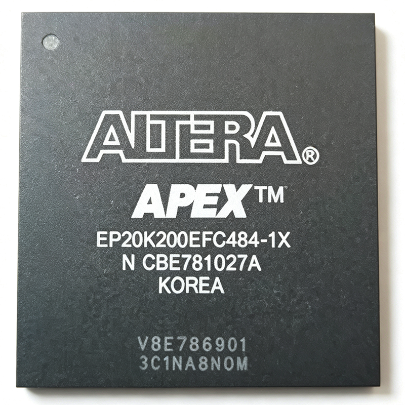
EP20K200EFC484-1X - 200K-Gate APEX 20KE FPGA | 484-FBGA | Intel
The Intel EP20K200EFC484-1X is a 200,000-gate APEX 20KE family Field Programmable Gate Array (FPGA) delivering 8,320 logic elements, 832 logic array blocks (LABs), and 106,496 bits of embedded RAM in a 484-ball FineLine BGA package. Built on a 0.22 µm CMOS process, it operates from a 1.71 V to 1.89 V core supply with up to 376 user I/O pins, supports propagation delays of approximately 2.5 ns, and is rated for the commercial 0 °C to 85 °C temperature window. An FPGA is a semiconductor device built around a matrix of configurable logic blocks (CLBs/LABs), programmable interconnect, and I/O cells that can be re-programmed in-system to implement arbitrary digital logic. FPGAs sit between fixed-function ASICs and software-defined processors in the design hierarchy: like an ASIC they implement hardware parallelism at full clock speed, but like a processor they can be re-spin in minutes by changing a bitstream. The APEX 20K family pioneered the MultiCore architecture that combined look-up-table (LUT) logic with embedded dual-port RAM and dedicated carry chains, enabling SOPC (System-On-A-Programmable-Chip) integration in the early 2000s. The 'E' suffix in APEX 20KE marks the enhanced variant with on-chip PLLs, LVDS I/O support, and a 4× speed-grade bump over the original APEX 20K family. The device integrates 106,496 bits of distributed RAM that can be configured as synchronous dual-port memory, FIFOs, or shift registers - a feature that allowed designers to replace external SRAM in many glue-logic and datapath applications. The 484-FBGA FineLine BGA package (23 × 23 mm) maximizes I/O count for high-pin-count designs while keeping the footprint manageable for four-layer PCB stack-ups. Typical applications for the EP20K200EFC484-1X include telecommunications line cards, custom datapath accelerators, bus-bridging glue logic, industrial control backplanes, and legacy ASIC prototyping where the design must remain bitstream-portable across Intel/Altera APEX 20K generations. Designers still target this part for long-life-cycle programs in industrial, aerospace, and defense where the APEX 20K bitstream is frozen and certification re-spins are costly. When designing with this FPGA, pay close attention to the multi-rail power architecture (VCCINT for core, VCCIO banks for I/O, VCC_PLL for PLL, VREF for reference voltages) and use a sequenced power supply to avoid latch-up. Use IBIS models for signal-architecture simulation because the 1.8 V core and LVTTL/LVCMOS I/O standards have very different switching characteristics. This page synthesizes distributor pricing, drop-in APEX 20K/20KE alternatives in the same 484-FBGA footprint, lifecycle context, and practical design notes not found in any single manufacturer datasheet.
EP20K200EFC484-2N - 200K Gate APEX-20KE FPGA, 484-FBGA | Intel
The Intel EP20K200EFC484-2N is a high-density APEX-20KE Field Programmable Gate Array (FPGA) delivering 200,000 system gates, 8,320 logic elements, and 106,496 bits of embedded RAM in a 484-pin FineLine BGA (FBGA) package. The device operates from a 1.8V core supply, supports up to 376 user I/O pins, and is built on a 0.22 µm CMOS MultiCore architecture that combines look-up table (LUT) logic with embedded memory blocks for true System-on-a-Programmable-Chip (SOPC) integration. An FPGA (Field Programmable Gate Array) is a semiconductor integrated circuit based on a matrix of configurable logic blocks (CLBs) connected via programmable interconnect, allowing hardware designers to implement custom digital logic without the cost of ASIC masks. Modern FPGAs sit in the hierarchy: programmable logic device (PLD) -> CPLD -> FPGA -> SoC FPGA (which adds hard processor cores), and belong to the broader category of programmable logic ICs. APEX-20KE is positioned as a high-density, system-level integration platform combining logic, memory, and dedicated I/O. Key differentiating features include 376 programmable I/Os supporting multiple I/O standards (LVTTL, LVCMOS, PCI, GTL+, SSTL), 4 embedded Phase-Locked Loops (PLLs) for clock management, and an embedded memory bandwidth of up to 200 MHz. The MultiCore architecture integrates LUT-based logic with embedded system blocks (ESBs), allowing designers to implement RAM, ROM, FIFO, and CAM functions without sacrificing logic capacity. The APEX-20KE architecture features a four-level hierarchical interconnect network (MegaLAB, LAB, FastTrack, and local interconnect), delivering predictable timing closure even in designs exceeding 100K gate equivalents. The 484-FBGA package with 1.0 mm ball pitch supports board-level integration while the 0.22 µm process balances logic density with I/O performance. Typical applications include telecommunications infrastructure (ATM switches, SONET/SDH framer ICs), high-speed data acquisition, digital signal processing pipelines, custom peripheral glue logic, and PCI bridge implementations. The 376 I/Os make it especially suitable for bus-intensive designs requiring parallel data paths. When designing with this FPGA, pay close attention to the I/O bank VCCIO configuration - mixing incompatible I/O standards on the same bank can damage the device. Use the Quartus II design software (or MAX+PLUS II for legacy projects) for synthesis and fitting; bitstream configuration is via the passive serial (PS), passive parallel async (PPA), or JTAG modes. This page synthesizes distributor stock and pricing, same-brand APEX-20K-family drop-in alternatives from the Site MPN list, and practical design notes not assembled in any single manufacturer datasheet.
EP20K200EFC484-2X - 200K-Gate APEX-20KE FPGA, 484-FBGA | Intel
The Intel (formerly Altera) EP20K200EFC484-2X is a 200,000-gate APEX-20KE family Field-Programmable Gate Array (FPGA) with 8,320 logic elements, 832 LABs/CLBs, and 106,496 bits of embedded RAM, housed in a 484-ball FineLine BGA package. It operates from a 1.71 V to 1.89 V core supply (1.8 V nominal) and exposes 376 user I/Os at a system frequency up to 205 MHz, fabricated on a 0.22 µm CMOS process. An FPGA is a programmable logic device (PLD) containing an array of configurable logic blocks (CLBs), embedded memory, routing interconnect, and I/O cells that engineers can program post-manufacture to implement arbitrary digital circuits. FPGAs sit in the broader semiconductor taxonomy as Application-Specific Integrated Circuit alternatives, below ASICs in NRE cost but above microcontrollers in parallel-processing throughput. The APEX-20KE family adds MultiCore interconnect and embedded ESB (Embedded System Block) memory to support system-on-a-programmable-chip (SOPC) designs. Key features of the EP20K200EFC484-2X include 8,320 logic elements (LEs), 106,496 total RAM bits organized as embedded system blocks, 376 maximum user I/Os, and a maximum operating frequency of 205 MHz. The -2X speed grade denotes a specific performance bin within the APEX-20KE family. The 484-FBGA (23x23 mm) FineLine BGA package provides high-density interconnect while remaining compatible with surface-mount PCB assembly lines. The device architecture combines four-input look-up tables (LUTs) per LE with MultiCore routing, embedded CAM, dual-port RAM, and content-addressable memory support. The 1.8 V core voltage reduces dynamic power compared to 2.5 V predecessors, and the I/O banks support multiple I/O standards including LVTTL, LVCMOS, and PCI. Typical applications include telecom line cards, industrial control logic, glue logic replacement, high-speed DSP pre-processing, and ASIC prototyping. The 200K-gate density is well matched to mid-complexity bus-bridging designs, video processing, and parallel interface aggregation. When designing with this part, ensure proper decoupling of all VCCINT and VCCIO rails and follow Altera AN 116 guidelines for APEX 20KE power-up sequencing. The 484-BGA package requires careful PCB layout with microvia technology for signal escape. This page synthesizes distributor pricing, drop-in pin-compatible alternatives, and practical design notes that supplement the manufacturer datasheet and reference designs.
EP20K200EFC672-2X - 200K Gates APEX 20KE FPGA, 672-FBGA | Intel
The Intel (formerly Altera) EP20K200EFC672-2X is a 200,000-gate APEX 20KE family FPGA featuring 8,320 logic elements and 376 user I/Os in a 672-ball FineLine BGA package. Built on a 0.22 µm CMOS process with 1.8 V core supply and MultiCore™ architecture, it integrates look-up table (LUT) logic with embedded system-on-a-programmable-chip (SOPC) memory blocks, targeting glue-logic replacement, custom datapath, and bus-interface bridging. An FPGA (Field-Programmable Gate Array) is a semiconductor device containing programmable logic blocks, interconnect, and I/O cells that the designer configures after manufacture. The APEX 20KE family sits within Intel's programmable-logic portfolio as a high-density, embedded-memory-rich family, hierarchically classified as FPGA -> programmable logic -> logic IC -> integrated circuit. The 'KE' suffix denotes enhanced on-chip memory and improved I/O support versus the original APEX 20K, while the embedded ESB (Embedded System Block) array allows each block to be configured as RAM, ROM, CAM, or multiplier. Key features of the EP20K200EFC672-2X include 8,320 logic cells, 832 macrocells, 376 maximum user I/Os, and 106,496 typical gates (200,000 maximum system gates). The device operates at a maximum internal frequency of 205 MHz and supports LVTTL, LVCMOS, PCI, SSTL, and GTL+ I/O standards. The 672-pin FineLine BGA package enables high signal-count designs in a compact footprint, suitable for backplane interfaces and high-speed parallel buses. The architecture combines four-input LUTs for combinational logic, dedicated carry chains for arithmetic, and a row/column interconnect optimized for data-path and memory-intensive designs. Four phase-locked loops (PLLs) provide clock multiplication and deskew, while the 1.8 V core reduces dynamic power relative to the 2.5 V APEX 20K predecessors. The device supports in-system programmability via JTAG and passive serial configuration, simplifying board-level bring-up. Typical applications include custom telecommunications backplane glue logic, PCI/PCI-X bus bridges, RAID controller datapaths, and legacy ASIC prototyping. The device also fits industrial control and imaging pipelines where parallel processing and embedded memory are required. Engineering teams evaluating long-life-cycle designs should note that the APEX 20KE family is no longer in active production and is supported primarily through authorized-stock distributors. When designing with the EP20K200EFC672-2X, ensure the Quartus design software version supports the APEX 20KE device family, as newer Quartus releases dropped legacy device support. Validate signal-integrity margins on the 672-ball FBGA fanout with BGA breakout routing rules, and confirm decoupling follows the manufacturer's reference-board power-distribution network guidelines. This page synthesizes distributor availability, parametric alternatives, and practical design notes not consolidated in the manufacturer datasheet, with values current as of 2026-09-07.
EP20K200EFI484-2X - APEX 20KE FPGA 200K Gates 484-FBGA | Intel
The Intel EP20K200EFI484-2X is a member of the APEX 20KE family of high-density Field-Programmable Gate Arrays (FPGAs) implementing 200,000 system gates, 8,320 logic elements, and 106,496 bits of embedded RAM in a 484-ball FineLine BGA package. Fabricated on a 0.22 µm CMOS process and operating from a 1.8 V core supply, the device exposes 376 user I/O pins and supports system-clock frequencies up to 205 MHz for high-throughput datapath designs. An FPGA (Field-Programmable Gate Array) is a reprogrammable logic device that combines configurable logic blocks, programmable interconnect, and embedded memory resources into a single semiconductor die. Within the broader semiconductor taxonomy, FPGAs sit between fixed-function ASICs and discrete glue logic, providing a programmable alternative for prototyping, low-volume production, and applications requiring late-stage design flexibility. The APEX 20KE family specifically introduced MultiCore architecture integrating look-up-table logic and embedded ESB (Embedded System Block) memory for system-on-a-programmable-chip (SOPC) integration. Key features include 376 user I/O pins supporting multiple I/O standards, embedded SRAM blocks totaling 106,496 bits for distributed data buffering, on-chip PLLs for clock multiplication and skew management, and JTAG-compliant IEEE 1149.1 boundary-scan test support. The FineLine BGA-484 thermally enhanced package provides mechanical robustness for demanding industrial environments and offers improved thermal dissipation versus standard BGA packaging. The APEX 20KE architecture combines Look-Up Table (LUT) based logic elements with embedded system blocks (ESBs), enabling designers to implement register-rich datapaths, FIFO memories, and dual-port RAM alongside conventional state machines. The MultiCore interconnect fabric delivers predictable timing closure, while the 0.22 µm CMOS process provides the speed grade headroom required for high-performance telecommunications and networking infrastructure designs. Typical applications include telecommunications line-card glue logic, industrial control and automation backplanes, ASIC prototyping for system validation, high-speed data acquisition front-ends, and military/aerospace signal-processing subsystems. The APEX 20KE family's wide I/O voltage tolerance and high pin count make it particularly suitable for bus-bridging applications where multiple legacy voltage domains must interoperate within a single board. When designing with this device, ensure proper decoupling of the 1.8 V core supply with bulk and high-frequency ceramic capacitors near the package. Configuration storage should use a serial or parallel PROM sized to the bitstream, and unused I/O pins must be configured as tri-stated inputs with pull-ups to avoid floating inputs on the board. This page synthesizes distributor stock and pricing data, pin-compatible APEX 20KE family alternatives, and practical design notes not consolidated on the manufacturer datasheet front page.
EP20K200EQC208-3 - APEX 20KE 200K Gate FPGA, 208-PQFP | Intel
The Intel (formerly Altera) EP20K200EQC208-3 is a member of the APEX 20KE family of Field Programmable Gate Arrays (FPGAs), delivering up to 200,000 system gates with 8,320 logic elements (LEs) and 106,496 embedded RAM bits in a 208-pin Plastic Quad Flat Pack (PQFP / 208-BFQFP) package. It belongs to the APEX-20KE series of SRAM-based, in-system programmable logic devices that combine look-up-table (LUT) logic with embedded memory and True-LVDS support. The speed grade suffix "-3" places this device in a moderate-performance bin suitable for general-purpose logic integration, glue logic replacement, and bus-interface bridging. An FPGA (Field Programmable Gate Array) is a semiconductor integrated circuit that can be configured by the customer after manufacturing using a hardware description language (HDL) and a vendor-specific toolchain. FPGAs sit within the broader category of programmable logic devices (PLDs), which historically evolved from simple PALs/GALs to complex CPLDs and then to SRAM-based FPGAs with embedded multipliers, memory blocks, and high-speed transceivers. APEX 20KE is positioned in the programmable-logic hypernymy tree as: FPGA -> SRAM-based FPGA -> LUT-based FPGA -> programmable logic device -> semiconductor IC. Engineers choose APEX 20KE for moderate-density glue-logic, bus bridges, and legacy system upgrades where software/firmware migration to newer families is undesirable. Key features of the EP20K200EQC208-3 include 136 user I/Os, a 2.5 V core supply (typical for the APEX 20KE generation), MultiVolt I/O support, embedded array blocks (EABs) for memory and DSP-style functions, in-system programmability via the IEEE 1149.1 JTAG interface, and CMOS low-power operation. The "E" suffix designates an enhanced variant that supports True-LVDS and additional I/O standards compared with the original APEX 20K. The "Q" in the package designator denotes a PQFP package, "C208" indicates 208 pins, and "-3" is the speed bin per the Altera/Intel APEX 20KE ordering code convention. The device uses a CMOS SRAM cell for configuration storage, which means the design must be loaded from an external configuration memory (EPC or compatible flash) at power-up via the Fast Passive Parallel (FPP), Passive Serial (PS), or JTAG configuration scheme. Embedded Array Blocks (EABs) implement dual-port RAM or ROM with widths up to 16 bits, enabling FIFO and lookup-table constructs. MultiVolt I/O allows interfacing with 1.8 V, 2.5 V, 3.3 V, and 5 V devices without external level shifters, which simplifies mixed-voltage board design. Typical applications for the EP20K200EQC208-3 include telecom line-card glue logic, industrial control interfaces, PCI/PCI-X bus bridges, printer imaging pipelines, network-attached storage controllers, and legacy equipment maintenance where the original APEX 20K design is being re-spun or extended. Its 136 user I/Os are sufficient for parallel buses, memory interfaces, and custom peripheral aggregation. Designers transitioning from APEX 20K to APEX 20KE gain additional I/O standards (LVDS, LVPECL) and improved timing closure without altering the PCB footprint if they stay within the same package. When designing with this FPGA, ensure the 208-PQFP land pattern is compatible with the chosen PCB library; the "E" variants are footprint-compatible with the original APEX 20K "Q" parts but include additional VREF and I/O-standard pins. Use Quartus II (version 13.0 or earlier; newer Quartus dropped APEX 20KE support) for synthesis, fitting, and timing analysis. Maintain a stable 2.5 V core rail with adequate decoupling (typically 0.1 µF and 10 µF bulk) and isolate configuration signals from noisy I/O traces. This page synthesizes distributor pricing (as of 2026-09-07), drop-in alternatives from the APEX 20K/20KE family and cross-brand reference data, and practical design notes not found in the standalone manufacturer datasheet PDF.