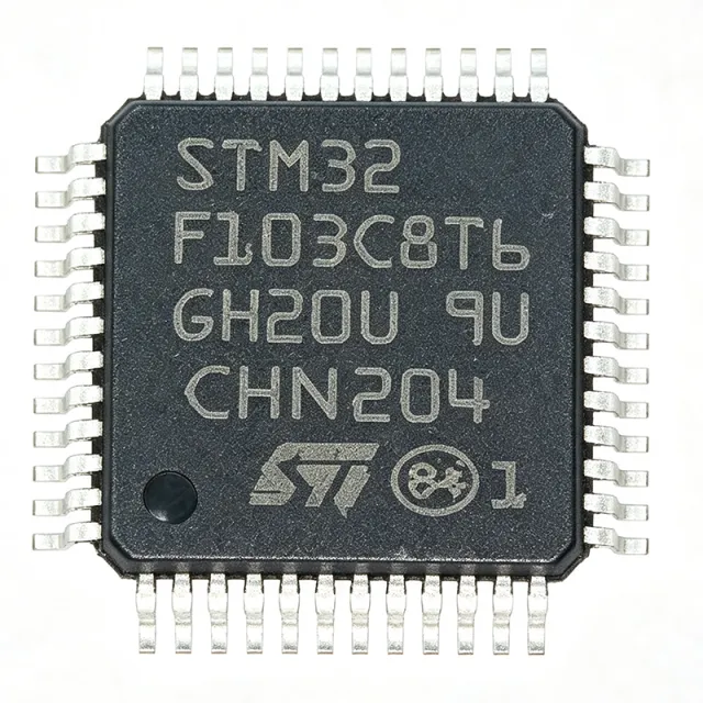
STM32F103C8T6 - 72MHz Cortex-M3 MCU, 64KB Flash, LQFP-48 | STMicroelectronics
Teilenummer: STM32F103C8T6 ✓ Aktiv| Menge | Stückpreis | Gesamt |
|---|---|---|
| 1 | $3.1 | $3,10 |
| 10 | $2.78 | $27,80 |
| 100 | $2.45 | $245,00 |
| 500 | $2.18 | $1.090,00 |
| 1.000 | $1.92 | $1.920,00 |
| 3.000 | $1.68 | $5.040,00 |
STM32F103C8T6 Übersicht
Ein ARM-Cortex-M3-Mikrocontroller (MCU) ist ein 32-Bit-RISC-Prozessorkern, der von Arm Holdings für Embedded-Anwendungen entwickelt wurde, die deterministische Echtzeitleistung bei geringem Stromverbrauch erfordern. Der Cortex-M3 liegt am unteren Ende der Cortex-M-Familie (über Cortex-M0/M0+ und unter Cortex-M4/M7), und Mikrocontroller dieser Kategorie kombinieren den Prozessorkern mit On-Chip-Speicher, Peripherie und analogen Blöcken zu einem einzigen System-on-Chip. Die STM32F103-Familie gehört konkret zur übergeordneten Hierarchie: ARM Cortex-M3 -> 32-Bit-MCU -> STM32F1-Serie -> STM32-Mainstream-Familie -> STMicroelectronics-Mikrocontroller -> Halbleiter. Diese Hierarchie ist wichtig, weil sie die Toolchain (Arm Cortex-M3 unterstützt die Standard-Flows Arm Keil, IAR, GCC und STM32CubeIDE) und das Peripherie-Programmiermodell bestimmt, das auf der gesamten STM32-Plattform verwendet wird.
Zu den Hauptmerkmalen gehören 64 KB eingebetteter Flash mit Read-While-Write-Fähigkeit, 20 KB SRAM, ein Versorgungsspannungsbereich von 2,0 V bis 3,6 V, ein interner 8-MHz-RC-Oszillator mit PLL-Multiplikator auf 72 MHz, zwei 12-Bit-ADCs (1 µs Wandlungszeit, bis zu 16 Kanäle), sieben 16-Bit-Timer und ein USB-2.0-Full-Speed-Device/Host/OTG-Controller. Zu den Kommunikationsperipherien gehören drei USARTs, zwei SPIs (18 Mbit/s), zwei I2C-Busse (400 kHz), eine CAN-2.0B-Schnittstelle und ein USB-Full-Speed-Port. Das 48-Pin-LQFP-Gehäuse stellt 37 GPIO-Pins bereit, die 5 V-tolerant sind.
Architektonisch liefert der Cortex-M3-Kern 1,25 Dhrystone MIPS pro MHz, unterstützt den Thumb-2-Befehlssatz und enthält einen Nested Vectored Interrupt Controller (NVIC) mit konfigurierbarer Priorität und Hardware-Stack-Verwaltung. Der integrierte Spannungsregler und der Brown-Out-Reset (BOR) vereinfachen das Stromversorgungsdesign, während das 4-Byte-Backup-Register mit Tamper-Detection-Pin batteriegepufferte RTC-Modi unterstützt.
Typische Anwendungen umfassen industrielle Steuerungsplatinen, Motorantriebe (BLDC/PMSM-FOC-Ergänzungen), USB-HID/COM-Port-Geräte, CAN-Bus-Knotenschnittstellen und kostengünstige Entwicklungsplattformen wie das bekannte "Blue Pill"-Board.
Beim Design mit diesem Baustein sollte ein 100-nF-Keramik-Entkopplungskondensator so nah wie möglich an jedem VDD/VDDA-Pin-Paar platziert und der NRST-Pin-Anschluss für einen 10-kΩ-Pull-up und einen optionalen Reset-Taster reserviert werden. Stellen Sie sicher, dass der BOOT0-Pin-Zustand bei jedem Einschalten dem gewünschten Boot-Speicher entspricht.
Diese Seite fasst Distributorpreise, Drop-in-Alternativen (zuerst STM32F103-Varianten derselben Marke, dann markenübergreifende pin-kompatible Teile) und praktische Designhinweise zusammen, die nicht im Herstellerdatenblatt zu finden sind.
Drop-in-Alternativen für STM32F103C8T6 – gleiches Gehäuse, Pin-kompatibel. Bauteile mit anderem Gehäuse, die eine PCB-Überarbeitung erfordern, sind ausgeschlossen.
Schnellvergleichstool – Wählen Sie Alternativbauteile für den Direktvergleich:
STM32F103CBT6
✓ Auf Lager
$3.2 / Stück
Datenblatt ansehen →STM32F030C8T6
✓ Auf Lager
$0.98 / Stück
Datenblatt ansehen →STM32F103C8T7
📋 Referenzalternative (nicht im Katalog)
GD32F103C8T6
📋 Referenzalternative (nicht im Katalog)
APM32F103C8T6
📋 Referenzalternative (nicht im Katalog)
STM32F103C8T6 Grenzwerte & elektrische Eigenschaften
| Core Architecture | ARM Cortex-M3 (32-bit RISC) |
| Maximale Taktfrequenz | 72 MHz |
| Flash Memory | 64 KB |
| SRAM | 20 KB |
| Supply Voltage (VDD) | 2.0 V to 3.6 V |
| Gehäuse | LQFP-48 (7x7 mm, 0.5 mm pitch) |
| GPIO Count | 37 |
| ADC | 2x 12-bit, 1 µs, up to 16 channels |
| Timers | 7x 16-bit (including 1x watchdog, 2x SysTick) |
| USART | 3 |
| SPI | 2 (18 Mbit/s) |
| I2C | 2 (400 kHz) |
| USB | 1x USB 2.0 Full-Speed device/host/OTG |
| CAN | 1x CAN 2.0B |
| Betriebstemperatur | -40 °C to +85 °C (industrial grade) |
| RoHS-Status | Compliant |
STM32F103C8T6 Pin-Konfiguration
| Pin 1 | VBAT — Backup battery supply input |
| Pin 2 | PC13 — GPIO PC13, anti-tamper (RTC) |
| Pin 3 | PC14 — GPIO PC14 / OSC32_IN |
| Pin 4 | PC15 — GPIO PC15 / OSC32_OUT |
| Pin 5 | OSC_IN — HSE oscillator input |
| Pin 6 | OSC_OUT — HSE oscillator output |
| Pin 7 | NRST — Reset input, active-low |
| Pin 8 | VSSA — Analog ground |
| Pin 9 | VDDA — Analog supply (2.4 V - 3.6 V) |
| Pin 10 | PA0 — GPIO PA0 / WKUP / ADC_IN0 / TIM2_CH1 |
| Pin 11 | PA1 — GPIO PA1 / ADC_IN1 / TIM2_CH2 |
| Pin 12 | PA2 — GPIO PA2 / USART2_TX / ADC_IN2 |
| Pin 13 | PA3 — GPIO PA3 / USART2_RX / ADC_IN3 |
| Pin 14 | PA4 — GPIO PA4 / SPI1_NSS / ADC_IN4 |
| Pin 15 | PA5 — GPIO PA5 / SPI1_SCK / ADC_IN5 |
| Pin 16 | PA6 — GPIO PA6 / SPI1_MISO / ADC_IN6 |
| Pin 17 | PA7 — GPIO PA7 / SPI1_MOSI / ADC_IN7 |
| Pin 18 | PB0 — GPIO PB0 / ADC_IN8 / TIM3_CH3 |
| Pin 19 | PB1 — GPIO PB1 / ADC_IN9 / TIM3_CH4 |
| Pin 20 | PB2 — GPIO PB2 / BOOT1 (also PB-BOOT input) |
| Pin 21 | PB10 — GPIO PB10 / I2C2_SCL / USART3_TX |
| Pin 22 | PB11 — GPIO PB11 / I2C2_SDA / USART3_RX |
| Pin 23 | VSS_1 — Digital ground |
| Pin 24 | VDD_1 — Digital supply (2.0 V - 3.6 V) |
| Pin 25 | PB12 — GPIO PB12 / SPI2_NSS / CAN2_RX |
| Pin 26 | PB13 — GPIO PB13 / SPI2_SCK / CAN2_TX / USB_DP pull-up |
| Pin 27 | PB14 — GPIO PB14 / SPI2_MISO |
| Pin 28 | PB15 — GPIO PB15 / SPI2_MOSI |
| Pin 29 | PA8 — GPIO PA8 / USART1_CK / TIM1_CH1 |
| Pin 30 | PA9 — GPIO PA9 / USART1_TX / TIM1_CH2 |
| Pin 31 | PA10 — GPIO PA10 / USART1_RX / TIM1_CH3 |
| Pin 32 | PA11 — GPIO PA11 / CAN1_RX / USBDM (USB data minus) |
| Pin 33 | PA12 — GPIO PA12 / CAN1_TX / USBDP (USB data plus) |
| Pin 34 | PA13 — GPIO PA13 / JTMS / SWDIO |
| Pin 35 | VSS_2 — Digital ground |
| Pin 36 | VDD_2 — Digital supply (2.0 V - 3.6 V) |
| Pin 37 | PA14 — GPIO PA14 / JTCK / SWCLK |
| Pin 38 | PA15 — GPIO PA15 / JTDI |
| Pin 39 | PB3 — GPIO PB3 / JTDO / TRACESWO |
| Pin 40 | PB4 — GPIO PB4 / JNTRST |
| Pin 41 | PB5 — GPIO PB5 / I2C1_SMBAI |
| Pin 42 | PB6 — GPIO PB6 / I2C1_SCL / TIM4_CH1 |
| Pin 43 | PB7 — GPIO PB7 / I2C1_SDA / TIM4_CH2 |
| Pin 44 | BOOT0 — Boot mode select (0 = Flash, 1 = System bootloader) |
| Pin 45 | PB8 — GPIO PB8 / TIM4_CH3 |
| Pin 46 | PB9 — GPIO PB9 / TIM4_CH4 |
| Pin 47 | VSS_3 — Digital ground |
| Pin 48 | VDD_3 — Digital supply (2.0 V - 3.6 V) |
Typische Anwendungen
STM32F103C8T6 ist geeignet für 6 Anwendungs: Industrial Control Boards, USB HID / Virtual COM Port Devices, BLDC / PMSM Motor Drives, CAN-Bus Node Interface, Low-Cost Development Platforms ("Blue Pill"), IoT Sensor / Smart Home Edge Nodes.
Industrial Control Boards
The STM32F103C8T6 fits industrial control boards because its 72 MHz Cortex-M3 core and 64 KB Flash comfortably handle Modbus RTU slave firmware, PID loop control, and user-interface logic on a single chip. The dual 12-bit ADCs (1 µs, up to 16 channels) sample 4-20 mA sensor inputs at the kHz rates typical of PLC analog modules, while the three USARTs (USART1/2/3) support simultaneous RS-232/RS-485 fieldbus and a debug console. The 2.0 V to 3.6 V supply range aligns with 3.3 V industrial backplanes, and the -40 °C to +85 °C operating temperature meets most cabinet-mounted equipment specs. On-board CAN 2.0B lets a single MCU handle both a sensor bus and an external CANopen master.
Empfohlen
USB HID / Virtual COM Port Devices
The STM32F103C8T6's integrated USB 2.0 Full-Speed device controller (12 Mbit/s) makes it a natural fit for USB HID-class peripherals, virtual COM-port bridges, and CDC-MSC composite devices without external PHY hardware. The 72 MHz core and 20 KB SRAM execute the standard ST USB device library (and STM32CubeMX-generated middleware) with room left for application logic, while the 64 KB Flash fits typical HID report descriptors and command parsers. Its 2.0 V to 3.6 V rail tolerance lets designers tap the USB 5 V bus through an LDO and run the MCU from a single 3.3 V supply. Designers should add ESD protection (USBLC6-2SC6) and a 1.5 kΩ pull-up on the D+ line to the USB connector.
Empfohlen
BLDC / PMSM Motor Drives
The STM32F103C8T6 is widely used in sensorless or hall-sensored BLDC and PMSM motor drives for low- to mid-power applications (fans, pumps, e-bike hubs). Its 72 MHz Cortex-M3 plus advanced timers (TIM1 with complementary PWM and dead-time insertion) generate the 6-step or space-vector PWM that drives a 3-phase inverter at up to tens of kHz switching. The two ADCs trigger from timer events to sample phase currents within the PWM cycle for low-latency commutation, and the quadrature encoder interface on TIM2 supports sensored FOC firmware patterns. CAN bus readiness lets the drive communicate with a central PLC, while the 2.0-3.6 V range accepts a wide range of bus-powered motor-control supplies.
Empfohlen
CAN-Bus Node Interface
The STM32F103C8T6 is a battle-tested choice for CAN 2.0B node interfaces used in automotive body-electronics, industrial CANopen, and medical device buses. The bxCAN peripheral supports standard and extended frames with hardware filter banks and a 1 Mbit/s bit rate suitable for most fieldbus deployments. With 64 KB Flash the device holds small CANopen/CANFestival stacks and application logic, while three USARTs allow a companion GPS or HMI link. Operating temperature of -40 °C to +85 °C suits non-automotive nodes; designers needing AEC-Q100 should select the STM32F103C8T7 variant. Drop a 60 Ω termination resistor only on the bus ends and add a TJA1050 or TCAN332 transceiver externally.
Empfohlen
Low-Cost Development Platforms ("Blue Pill")
The STM32F103C8T6 is the headline MCU of the iconic "Blue Pill" development board that became the de-facto entry ticket to ARM Cortex-M3 firmware development. Its 72 MHz core, 64 KB Flash, SWD debug pins, USB connector, and 48-pin LQFP form factor fit on a 53 x 23 mm PCB with a USB micro-B port, a 3.3 V LDO, a reset button, and boot-mode jumpers. Students and hobbyists target it with STM32CubeIDE, PlatformIO, and the Arduino STM32 core, and any prototype firmware written on the Blue Pill ports directly to custom hardware when the same MCU is kept on the production board. The LQFP-48 footprint is also shared by several GD32 and APM32 pin-compatibles, simplifying second sourcing for educational kits.
Empfohlen
IoT Sensor / Smart Home Edge Nodes
The STM32F103C8T6 handles Smart Home and IoT edge nodes that need local sensor aggregation, BLE/Wi-Fi module handshaking, and OTA bootloading without committing to a high-cost M4-class part. Three USARTs (USART1/2/3) drive an ESP-01 Wi-Fi co-processor, a GPS module, and a debug console in parallel; two SPIs (up to 18 Mbit/s) talk to a LoRa SX1278 or a small TFT display; two I2C buses serve a BME280 environmental sensor and an OLED panel. The 12-bit ADC samples analog sensors such as soil-moisture probes, and the RTC plus 4-byte backup register keep a wall-clock time across deep-sleep cycles powered by a CR2032. The 2.0-3.6 V supply range supports direct lithium-ion battery operation via an LDO or buck.
Empfohlen
Zusammenfassung der empfohlenen Produkte
Technische Referenzdaten für STM32F103C8T6 – Vergleich, Designhinweise und Compliance-Informationen.
Auswahlhilfe
Vergleich mit Alternativen
| Parameter | Dieses Produkt | STM32F103CBT6 | STM32F103C8T7 | GD32F103C8T6 | APM32F103C8T6 | STM32F030C8T6 |
|---|---|---|---|---|---|---|
| Brand | STMicroelectronics | STMicroelectronics | STMicroelectronics | GigaDevice | GigaDevice | STMicroelectronics |
| Package | LQFP-48 (7x7 mm) | LQFP-48 (7x7 mm) - same | LQFP-48 (7x7 mm) - same | LQFP-48 (7x7 mm) - same | LQFP-48 (7x7 mm) - same | LQFP-48 (7x7 mm) - same |
| Core | ARM Cortex-M3 | ARM Cortex-M3 | ARM Cortex-M3 | ARM Cortex-M3 | ARM Cortex-M3 | ARM Cortex-M0 (-1 class) |
| Max Clock | 72 MHz | 72 MHz | 72 MHz | 108 MHz (+50%) | 96 MHz (+33%) | 48 MHz (-33%) |
| Flash | 64 KB | 128 KB (+100%) | 64 KB | 64 KB | 64 KB | 64 KB |
| SRAM | 20 KB | 20 KB | 20 KB | 20 KB | 20 KB | 8 KB (-60%) |
| USB | USB 2.0 Full-Speed | USB 2.0 Full-Speed | USB 2.0 Full-Speed | USB 2.0 Full-Speed | USB 2.0 Full-Speed | No USB |
| CAN | 1x CAN 2.0B | 1x CAN 2.0B | 1x CAN 2.0B | 1x CAN 2.0B | 1x CAN 2.0B | No CAN |
| Automotive Grade | No (industrial -40/+85C) | No | Yes (AEC-Q100) | No | No | No |
Wichtigste Unterscheidungsmerkmale
- Pin-kompatibler Drop-in mit doppeltem Flash innerhalb derselben Familie (vs. STM32F103CBT6)
- AEC-Q100-Automotive-Temperaturgrad auf demselben Silizium/Die verfügbar (vs. STM32F103C8T7)
- Zwei- bis viermal schnellerer Kern auf demselben LQFP-48-Footprint (vs. GD32F103C8T6)
Designhinweise
Platzieren Sie 100-nF-Keramik-Entkopplungskondensatoren so nah wie möglich an jedem VDD/VDDA-Pin-Paar (Pins 24, 36, 48 / 9), mit mindestens einem Bulk-Kondensator von 4,7 µF auf der Haupt-3,3-V-Schiene innerhalb von 20 mm. VDDA erfordert eine niederimpedante Verbindung; wenn die Haupt-3,3-V-Versorgung verrauscht ist, fügen Sie eine Ferritperle zwischen VDD und VDDA ein. Verbinden Sie VBAT mit VDD, wenn keine Backup-Batterie verwendet wird. Halten Sie den BOOT0-Pin beim Einschalten immer auf Low, um standardmäßig aus dem Flash zu booten.
Führen Sie die 8-MHz-HSE-Quarzleitungen kurz und symmetrisch, platzieren Sie den Quarz innerhalb von 5 mm von OSC_IN/OSC_OUT (Pins 5/6) und erden Sie die Lastkondensatoren (typischerweise 20-30 pF) direkt am Quarzgehäuse. Halten Sie USB D+/D- (PA11/PA12) längengleich (Ziel <2 mm Delta) und platzieren Sie den 1,5-kΩ-Pull-up an D+ neben dem Stecker, nicht auf der MCU-Seite. Stellen Sie einen 10-kΩ-Pull-up an NRST und einen niederimpedanten Pfad zu GND über einen Reset-Taster bereit.
Fügen Sie bei Verwendung von CAN oder USB ein TVS-Diodenarray wie USBLC6-2SC6 oder PESD1CAN nahe am Stecker hinzu, um die IEC 61000-4-2 ±8 kV Luftentladung und ±4 kV Kontaktentladung zu erfüllen. Der interne Pull-up an USB D+ (PA12) ist nicht stark genug für eine zuverlässige Enumeration; ein externer 1,5-kΩ-Widerstand nach 3,3 V wird empfohlen. Die CAN-Bus-Terminierung sollte nur an beiden Enden 120 Ω verwenden, mit einem Split-Kondensator-Netzwerk zur Stichleitungsunterdrückung in Mehrknoten-Kabelbäumen.
Lassen Sie BOOT0 nicht floaten - Rauschen auf diesem Pin während des Einschaltens bootet die MCU sporadisch in den System-Bootloader und der Anwendungscode scheint zu fehlen. Drei häufige Fehler: (1) VBAT floaten lassen statt es mit VDD zu verbinden, was die interne Diode lädt und Backup-Register-Schreibvorgänge korrumpiert; (2) PA13/PA14 als GPIO verwenden, ohne JTAG/SWD zu deaktivieren, da JTAG nach dem Reset standardmäßig diese Pins belegt; (3) die GPIO-Ausgangsgeschwindigkeit auf I2C-Pins auf '50 MHz' konfigurieren, was Ringing verursacht - wählen Sie immer '2 MHz' Open-Drain mit externen Pull-ups.
Compliance-Informationen
RoHS-compliant per ST product page; AEC-Q100 grade is a separate SKU (STM32F103C8T7). Halogen-free status not explicitly verified in the provided data and flagged as 'unknown'.







