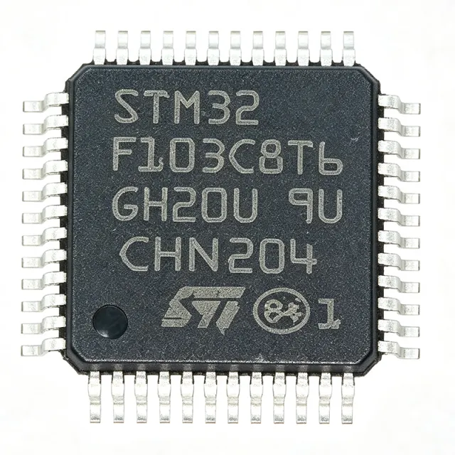
STM32F103C8T6 - MCU Cortex-M3 de 72MHz, 64KB de Flash, LQFP-48 | STMicroelectronics
N.º de pieza: STM32F103C8T6 ✓ Activo| Cant. | Precio unitario | Total |
|---|---|---|
| 1 | $3.1 | $3,10 |
| 10 | $2.78 | $27,80 |
| 100 | $2.45 | $245,00 |
| 500 | $2.18 | $1.090,00 |
| 1.000 | $1.92 | $1.920,00 |
| 3.000 | $1.68 | $5.040,00 |
STM32F103C8T6 Descripción general
Un microcontrolador (MCU) ARM Cortex-M3 es un núcleo de procesador RISC de 32 bits diseñado por Arm Holdings para aplicaciones embebidas que requieren un rendimiento determinista en tiempo real con bajo consumo. El Cortex-M3 se sitúa en el extremo inferior de la familia Cortex-M (por encima del Cortex-M0/M0+ y por debajo del Cortex-M4/M7), y los microcontroladores de esta categoría combinan el núcleo del procesador con memoria integrada, periféricos y bloques analógicos en un único sistema en chip. La familia STM32F103 pertenece específicamente a la jerarquía más amplia: ARM Cortex-M3 -> MCU de 32 bits -> serie STM32F1 -> familia principal STM32 -> microcontroladores STMicroelectronics -> semiconductor. Esta jerarquía es importante porque determina la cadena de herramientas (Arm Cortex-M3 admite los flujos estándar de Arm Keil, IAR, GCC y STM32CubeIDE) y el modelo de programación de periféricos utilizado en toda la plataforma STM32.
Las características clave incluyen 64 KB de Flash integrada con capacidad de lectura mientras se escribe, 20 KB de SRAM, un rango de alimentación de 2,0 V a 3,6 V, un oscilador RC interno de 8 MHz con multiplicador PLL hasta 72 MHz, dos ADC de 12 bits (conversión de 1 µs, hasta 16 canales), siete temporizadores de 16 bits y un controlador USB 2.0 Full-Speed de dispositivo/host/OTG. Los periféricos de comunicación incluyen tres USART, dos SPI (18 Mbit/s), dos buses I2C (400 kHz), una interfaz CAN 2.0B y un puerto USB Full-Speed. El encapsulado LQFP de 48 pines expone 37 pines GPIO tolerantes a 5 V.
Arquitectónicamente, el núcleo Cortex-M3 ofrece 1,25 Dhrystone MIPS por MHz, admite el conjunto de instrucciones Thumb-2 e incluye un controlador de interrupciones vectorizadas anidadas (NVIC) con prioridad configurable y manejo de pila por hardware. El regulador de tensión integrado y el reset por caída de tensión (BOR) simplifican el diseño de alimentación, mientras que el registro de respaldo de 4 bytes con un pin de detección de manipulación admite modos RTC con respaldo por batería.
Las aplicaciones típicas incluyen placas de control industrial, accionamientos de motores (complementos FOC para BLDC/PMSM), dispositivos USB HID/puerto COM, interfaces de nodo de bus CAN y plataformas de desarrollo de bajo costo como la conocida placa "Blue Pill".
Al diseñar con este dispositivo, coloque un condensador cerámico de desacoplo de 100 nF lo más cerca posible de cada par de pines VDD/VDDA, y reserve la conexión del pin NRST para una resistencia pull-up de 10 kΩ y un botón de reset opcional. Asegúrese de que el estado del pin BOOT0 coincida con la memoria de arranque deseada en cada encendido.
Esta página sintetiza los precios de distribuidores, las alternativas de reemplazo directo (primero las variantes STM32F103 de la misma marca, luego las piezas compatibles en pines de otras marcas) y notas de diseño prácticas que no se encuentran en la hoja de datos del fabricante.
Alternativas directas para STM32F103C8T6 — mismo encapsulado, compatible pin a pin. Se excluyen las piezas de otro encapsulado que requieren retrabajo de la PCB.
Herramienta de comparación rápida — seleccione piezas alternativas para compararlas lado a lado:
STM32F103CBT6
✓ En stock
$3.2 / unidad
Ver hoja de datos →STM32F030C8T6
✓ En stock
$0.98 / unidad
Ver hoja de datos →STM32F103C8T7
📋 Alternativa de referencia (no en el catálogo)
GD32F103C8T6
📋 Alternativa de referencia (no en el catálogo)
APM32F103C8T6
📋 Alternativa de referencia (no en el catálogo)
STM32F103C8T6 Valores máximos y características eléctricas
| Core Architecture | ARM Cortex-M3 (32-bit RISC) |
| Frecuencia de reloj máxima | 72 MHz |
| Flash Memory | 64 KB |
| SRAM | 20 KB |
| Supply Voltage (VDD) | 2.0 V to 3.6 V |
| Encapsulado | LQFP-48 (7x7 mm, 0.5 mm pitch) |
| GPIO Count | 37 |
| ADC | 2x 12-bit, 1 µs, up to 16 channels |
| Timers | 7x 16-bit (including 1x watchdog, 2x SysTick) |
| USART | 3 |
| SPI | 2 (18 Mbit/s) |
| I2C | 2 (400 kHz) |
| USB | 1x USB 2.0 Full-Speed device/host/OTG |
| CAN | 1x CAN 2.0B |
| Temperatura de funcionamiento | -40 °C to +85 °C (industrial grade) |
| Estado RoHS | Compliant |
Configuración de pines de STM32F103C8T6
| Pin 1 | VBAT — Backup battery supply input |
| Pin 2 | PC13 — GPIO PC13, anti-tamper (RTC) |
| Pin 3 | PC14 — GPIO PC14 / OSC32_IN |
| Pin 4 | PC15 — GPIO PC15 / OSC32_OUT |
| Pin 5 | OSC_IN — HSE oscillator input |
| Pin 6 | OSC_OUT — HSE oscillator output |
| Pin 7 | NRST — Reset input, active-low |
| Pin 8 | VSSA — Analog ground |
| Pin 9 | VDDA — Analog supply (2.4 V - 3.6 V) |
| Pin 10 | PA0 — GPIO PA0 / WKUP / ADC_IN0 / TIM2_CH1 |
| Pin 11 | PA1 — GPIO PA1 / ADC_IN1 / TIM2_CH2 |
| Pin 12 | PA2 — GPIO PA2 / USART2_TX / ADC_IN2 |
| Pin 13 | PA3 — GPIO PA3 / USART2_RX / ADC_IN3 |
| Pin 14 | PA4 — GPIO PA4 / SPI1_NSS / ADC_IN4 |
| Pin 15 | PA5 — GPIO PA5 / SPI1_SCK / ADC_IN5 |
| Pin 16 | PA6 — GPIO PA6 / SPI1_MISO / ADC_IN6 |
| Pin 17 | PA7 — GPIO PA7 / SPI1_MOSI / ADC_IN7 |
| Pin 18 | PB0 — GPIO PB0 / ADC_IN8 / TIM3_CH3 |
| Pin 19 | PB1 — GPIO PB1 / ADC_IN9 / TIM3_CH4 |
| Pin 20 | PB2 — GPIO PB2 / BOOT1 (also PB-BOOT input) |
| Pin 21 | PB10 — GPIO PB10 / I2C2_SCL / USART3_TX |
| Pin 22 | PB11 — GPIO PB11 / I2C2_SDA / USART3_RX |
| Pin 23 | VSS_1 — Digital ground |
| Pin 24 | VDD_1 — Digital supply (2.0 V - 3.6 V) |
| Pin 25 | PB12 — GPIO PB12 / SPI2_NSS / CAN2_RX |
| Pin 26 | PB13 — GPIO PB13 / SPI2_SCK / CAN2_TX / USB_DP pull-up |
| Pin 27 | PB14 — GPIO PB14 / SPI2_MISO |
| Pin 28 | PB15 — GPIO PB15 / SPI2_MOSI |
| Pin 29 | PA8 — GPIO PA8 / USART1_CK / TIM1_CH1 |
| Pin 30 | PA9 — GPIO PA9 / USART1_TX / TIM1_CH2 |
| Pin 31 | PA10 — GPIO PA10 / USART1_RX / TIM1_CH3 |
| Pin 32 | PA11 — GPIO PA11 / CAN1_RX / USBDM (USB data minus) |
| Pin 33 | PA12 — GPIO PA12 / CAN1_TX / USBDP (USB data plus) |
| Pin 34 | PA13 — GPIO PA13 / JTMS / SWDIO |
| Pin 35 | VSS_2 — Digital ground |
| Pin 36 | VDD_2 — Digital supply (2.0 V - 3.6 V) |
| Pin 37 | PA14 — GPIO PA14 / JTCK / SWCLK |
| Pin 38 | PA15 — GPIO PA15 / JTDI |
| Pin 39 | PB3 — GPIO PB3 / JTDO / TRACESWO |
| Pin 40 | PB4 — GPIO PB4 / JNTRST |
| Pin 41 | PB5 — GPIO PB5 / I2C1_SMBAI |
| Pin 42 | PB6 — GPIO PB6 / I2C1_SCL / TIM4_CH1 |
| Pin 43 | PB7 — GPIO PB7 / I2C1_SDA / TIM4_CH2 |
| Pin 44 | BOOT0 — Boot mode select (0 = Flash, 1 = System bootloader) |
| Pin 45 | PB8 — GPIO PB8 / TIM4_CH3 |
| Pin 46 | PB9 — GPIO PB9 / TIM4_CH4 |
| Pin 47 | VSS_3 — Digital ground |
| Pin 48 | VDD_3 — Digital supply (2.0 V - 3.6 V) |
Aplicaciones típicas
STM32F103C8T6 es adecuado para 6 aplicacións: Industrial Control Boards, USB HID / Virtual COM Port Devices, BLDC / PMSM Motor Drives, CAN-Bus Node Interface, Low-Cost Development Platforms ("Blue Pill"), IoT Sensor / Smart Home Edge Nodes.
Industrial Control Boards
The STM32F103C8T6 fits industrial control boards because its 72 MHz Cortex-M3 core and 64 KB Flash comfortably handle Modbus RTU slave firmware, PID loop control, and user-interface logic on a single chip. The dual 12-bit ADCs (1 µs, up to 16 channels) sample 4-20 mA sensor inputs at the kHz rates typical of PLC analog modules, while the three USARTs (USART1/2/3) support simultaneous RS-232/RS-485 fieldbus and a debug console. The 2.0 V to 3.6 V supply range aligns with 3.3 V industrial backplanes, and the -40 °C to +85 °C operating temperature meets most cabinet-mounted equipment specs. On-board CAN 2.0B lets a single MCU handle both a sensor bus and an external CANopen master.
Recomendado
USB HID / Virtual COM Port Devices
The STM32F103C8T6's integrated USB 2.0 Full-Speed device controller (12 Mbit/s) makes it a natural fit for USB HID-class peripherals, virtual COM-port bridges, and CDC-MSC composite devices without external PHY hardware. The 72 MHz core and 20 KB SRAM execute the standard ST USB device library (and STM32CubeMX-generated middleware) with room left for application logic, while the 64 KB Flash fits typical HID report descriptors and command parsers. Its 2.0 V to 3.6 V rail tolerance lets designers tap the USB 5 V bus through an LDO and run the MCU from a single 3.3 V supply. Designers should add ESD protection (USBLC6-2SC6) and a 1.5 kΩ pull-up on the D+ line to the USB connector.
Recomendado
BLDC / PMSM Motor Drives
The STM32F103C8T6 is widely used in sensorless or hall-sensored BLDC and PMSM motor drives for low- to mid-power applications (fans, pumps, e-bike hubs). Its 72 MHz Cortex-M3 plus advanced timers (TIM1 with complementary PWM and dead-time insertion) generate the 6-step or space-vector PWM that drives a 3-phase inverter at up to tens of kHz switching. The two ADCs trigger from timer events to sample phase currents within the PWM cycle for low-latency commutation, and the quadrature encoder interface on TIM2 supports sensored FOC firmware patterns. CAN bus readiness lets the drive communicate with a central PLC, while the 2.0-3.6 V range accepts a wide range of bus-powered motor-control supplies.
Recomendado
CAN-Bus Node Interface
The STM32F103C8T6 is a battle-tested choice for CAN 2.0B node interfaces used in automotive body-electronics, industrial CANopen, and medical device buses. The bxCAN peripheral supports standard and extended frames with hardware filter banks and a 1 Mbit/s bit rate suitable for most fieldbus deployments. With 64 KB Flash the device holds small CANopen/CANFestival stacks and application logic, while three USARTs allow a companion GPS or HMI link. Operating temperature of -40 °C to +85 °C suits non-automotive nodes; designers needing AEC-Q100 should select the STM32F103C8T7 variant. Drop a 60 Ω termination resistor only on the bus ends and add a TJA1050 or TCAN332 transceiver externally.
Recomendado
Low-Cost Development Platforms ("Blue Pill")
The STM32F103C8T6 is the headline MCU of the iconic "Blue Pill" development board that became the de-facto entry ticket to ARM Cortex-M3 firmware development. Its 72 MHz core, 64 KB Flash, SWD debug pins, USB connector, and 48-pin LQFP form factor fit on a 53 x 23 mm PCB with a USB micro-B port, a 3.3 V LDO, a reset button, and boot-mode jumpers. Students and hobbyists target it with STM32CubeIDE, PlatformIO, and the Arduino STM32 core, and any prototype firmware written on the Blue Pill ports directly to custom hardware when the same MCU is kept on the production board. The LQFP-48 footprint is also shared by several GD32 and APM32 pin-compatibles, simplifying second sourcing for educational kits.
Recomendado
IoT Sensor / Smart Home Edge Nodes
The STM32F103C8T6 handles Smart Home and IoT edge nodes that need local sensor aggregation, BLE/Wi-Fi module handshaking, and OTA bootloading without committing to a high-cost M4-class part. Three USARTs (USART1/2/3) drive an ESP-01 Wi-Fi co-processor, a GPS module, and a debug console in parallel; two SPIs (up to 18 Mbit/s) talk to a LoRa SX1278 or a small TFT display; two I2C buses serve a BME280 environmental sensor and an OLED panel. The 12-bit ADC samples analog sensors such as soil-moisture probes, and the RTC plus 4-byte backup register keep a wall-clock time across deep-sleep cycles powered by a CR2032. The 2.0-3.6 V supply range supports direct lithium-ion battery operation via an LDO or buck.
Recomendado
Resumen de productos recomendados
Datos de referencia de ingeniería para STM32F103C8T6 — comparación, orientación de diseño e información de cumplimiento.
Guía de selección
Comparación con alternativas
| Parámetro | Este producto | STM32F103CBT6 | STM32F103C8T7 | GD32F103C8T6 | APM32F103C8T6 | STM32F030C8T6 |
|---|---|---|---|---|---|---|
| Brand | STMicroelectronics | STMicroelectronics | STMicroelectronics | GigaDevice | GigaDevice | STMicroelectronics |
| Package | LQFP-48 (7x7 mm) | LQFP-48 (7x7 mm) - same | LQFP-48 (7x7 mm) - same | LQFP-48 (7x7 mm) - same | LQFP-48 (7x7 mm) - same | LQFP-48 (7x7 mm) - same |
| Core | ARM Cortex-M3 | ARM Cortex-M3 | ARM Cortex-M3 | ARM Cortex-M3 | ARM Cortex-M3 | ARM Cortex-M0 (-1 class) |
| Max Clock | 72 MHz | 72 MHz | 72 MHz | 108 MHz (+50%) | 96 MHz (+33%) | 48 MHz (-33%) |
| Flash | 64 KB | 128 KB (+100%) | 64 KB | 64 KB | 64 KB | 64 KB |
| SRAM | 20 KB | 20 KB | 20 KB | 20 KB | 20 KB | 8 KB (-60%) |
| USB | USB 2.0 Full-Speed | USB 2.0 Full-Speed | USB 2.0 Full-Speed | USB 2.0 Full-Speed | USB 2.0 Full-Speed | No USB |
| CAN | 1x CAN 2.0B | 1x CAN 2.0B | 1x CAN 2.0B | 1x CAN 2.0B | 1x CAN 2.0B | No CAN |
| Automotive Grade | No (industrial -40/+85C) | No | Yes (AEC-Q100) | No | No | No |
Diferenciadores clave
- Reemplazo directo compatible en pines con Flash duplicada dentro de la misma familia (frente a STM32F103CBT6)
- Grado de temperatura automotriz AEC-Q100 disponible en el mismo silicio/die (frente a STM32F103C8T7)
- Núcleo de dos a cuatro veces más rápido en la misma huella LQFP-48 (frente a GD32F103C8T6)
Notas de diseño
Coloque condensadores cerámicos de desacoplo de 100 nF lo más cerca posible de cada par de pines VDD/VDDA (pines 24, 36, 48 / 9), con al menos un condensador de masa de 4,7 µF en el riel principal de 3,3 V a menos de 20 mm. VDDA requiere una conexión de baja impedancia; si la alimentación principal de 3,3 V es ruidosa, inserte una ferrita entre VDD y VDDA. Conecte VBAT a VDD si no se utiliza una batería de respaldo. Mantenga siempre el pin BOOT0 en bajo al encender para arrancar por defecto desde la Flash.
Rutee las pistas del cristal HSE de 8 MHz cortas y simétricas, con el cristal colocado a menos de 5 mm de OSC_IN/OSC_OUT (pines 5/6) y los condensadores de carga (típicamente 20-30 pF) conectados a tierra justo en la carcasa del cristal. Mantenga USB D+/D- (PA11/PA12) con longitud igualada (objetivo <2 mm de diferencia) y coloque la resistencia pull-up de 1,5 kΩ en D+ junto al conector, no del lado del MCU. Proporcione una pull-up de 10 kΩ en NRST y una ruta de baja impedancia a GND a través de un pulsador de reset.
Cuando utilice CAN o USB, agregue un arreglo de diodos TVS como USBLC6-2SC6 o PESD1CAN cerca del conector para cumplir con las clasificaciones IEC 61000-4-2 de ±8 kV descarga de aire y ±4 kV descarga por contacto. La pull-up interna en USB D+ (PA12) no es suficientemente fuerte para una enumeración confiable; se recomienda una resistencia externa de 1,5 kΩ a 3,3 V. La terminación del bus CAN debe usar 120 Ω solo en ambos extremos, con una red de condensador dividido para supresión de derivaciones en arneses de múltiples nodos.
No deje BOOT0 flotando: el ruido en este pin durante el encendido hará que el MCU arranque intermitentemente en el bootloader del sistema y el código de la aplicación parecerá faltar. Tres errores comunes: (1) dejar VBAT flotando en lugar de conectarlo a VDD, lo que carga el diodo interno y corrompe las escrituras del registro de respaldo; (2) usar PA13/PA14 como GPIO sin deshabilitar JTAG/SWD, ya que JTAG usa estos pines por defecto después del reset; (3) configurar la velocidad de salida GPIO a '50 MHz' en los pines I2C, lo que causa ringing: seleccione siempre '2 MHz' en drenador abierto con pull-ups externas.
Información de cumplimiento
RoHS-compliant per ST product page; AEC-Q100 grade is a separate SKU (STM32F103C8T7). Halogen-free status not explicitly verified in the provided data and flagged as 'unknown'.







