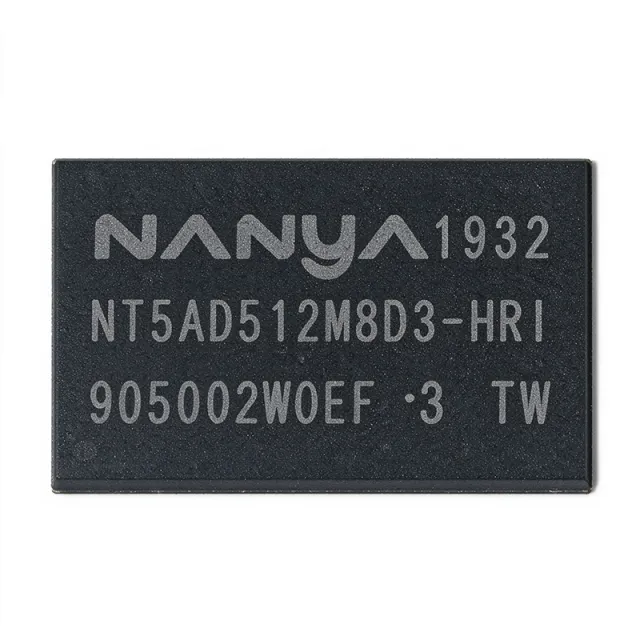
NT5AD512M16C4-HRI - 8Gb DDR4 SDRAM 512Mx16 | Nanya Technology
MPN: NT5AD512M16C4-HRI ✓ Aktif| Kwantitas | Harga Satuan | Lengkap |
|---|---|---|
| 1 | $78.75 | $78,75 |
| 10 | $56.875 | $568,75 |
| 100 | $50.3125 | $5.031,25 |
| 500 | $48.125 | $24.062,50 |
| 1.000 | $45.9375 | $45.937,50 |
NT5AD512M16C4-HRI Ringkasan
DDR4 SDRAM (Double Data Rate 4 Synchronous Dynamic Random-Access Memory) is a type of volatile memory that transfers data on both edges of the clock signal, doubling the data rate compared to DDR3. It features a prefetch buffer of 8n, allowing high-speed data access while maintaining lower operating voltages (1.2V vs 1.5V for DDR3), which reduces power consumption and heat generation. DDR4 is the industry standard for modern computing, networking, and embedded systems, offering improved reliability and performance over previous generations.
Key features of the NT5AD512M16C4-HRI include an industrial temperature grade (0°C to +95°C), auto self-refresh, built-in temperature sensor, auto precharge, asynchronous reset, data mask, write leveling, dynamic on-chip termination (ODT), ZQ calibration, and CRC (Cyclic Redundancy Check) function. These features enhance signal integrity, data reliability, and system robustness, particularly in demanding industrial environments.
The device supports data rates up to 3200 MT/s (per the 'H' speed grade), with a CAS latency of 22 cycles. It utilizes a 16n prefetch architecture and includes on-die ECC for improved data integrity. The 96-ball TFBGA package measures 9mm x 13mm with a 0.8mm ball pitch, offering excellent thermal and electrical performance for high-speed operation.
Typical applications include industrial controllers, embedded computing modules, networking equipment, and data storage systems. The industrial temperature range and robust feature set make it ideal for applications requiring reliable operation in harsh environments, such as factory automation, transportation, and outdoor infrastructure.
When designing with this DDR4 device, ensure proper termination and layout practices are followed to maintain signal integrity at high speeds. The ZQ calibration pin requires a 240-ohm resistor to ground, and the VTT and VREF supplies must be properly decoupled. Refer to the Nanya datasheet for detailed PCB layout guidelines and timing parameters.
Alternatif penggantian untuk NT5AD512M16C4-HRI — paket yang sama, pin-pada-pin kompatibel. Bagian paket yang berbeda memerlukan kerja ulang PCB diabaikan.
Variasi di dalam seri ini
Model-series yang sama yang kompatibel dengan penggantian NT5AD512M16C4-HRI (sama faktor bentuk dan footprint) — berbeda di dalam Data Rate, Package.
Alat Perbandingan Cepat — Pilih bagian alternatif untuk perbandingan paralel:
NT5AD512M16C4-JRI
✓ Ada di Gudang
$75.58 / Satuan
Lihat Datasheet →NT5AD512M16C4-HR
Kontak untuk harga
Lihat Datasheet →NT5AD512M16C4-JR
✗ Habis Stok
$73.75 / Satuan
Lihat Datasheet →MT40A512M16TB-062E
✗ Habis Stok
$60 / Satuan
Lihat Datasheet →K4A8G165WC-BCWE
✗ Habis Stok
$38 / Satuan
Lihat Datasheet →H5AN8G6NCJR-VKC
✗ Habis Stok
$60 / Satuan
Lihat Datasheet →NT5AD512M16C4-HRI Rating Maksimal & Karakteristik Listrik
| Tipe Memori | DDR4 SDRAM |
| Organisasi | 512M x 16 |
| Density | 8 Gbit |
| Tegangan Pemuat | 1.2 V |
| Paket | 96-pin TFBGA |
| Temperature Grade | Industrial (0°C to +95°C) |
| Laju Data | 3200 MT/s (H speed grade) |
| Latensi CAS | 22 |
| Auto Self-Refresh | Yes |
| Built-in Temperature Sensor | Yes |
| Auto Precharge | Yes |
| Asynchronous Reset | Yes |
| Data Mask | Yes |
| Write Leveling | Yes |
| Dynamic On-Chip Termination | Yes |
| ZQ Calibration | Yes |
| CRC Function | Yes |
| RoHS | Compliant |
Konfigurasi Pin NT5AD512M16C4-HRI
| Pin produk A1 | VDD — Power supply (1.2V) |
| Pin produk A2 | DQ0 — Data input/output 0 |
| Pin produk A3 | DQ1 — Data input/output 1 |
| Pin produk A4 | VSS — Ground |
| Pin produk A5 | DQ2 — Data input/output 2 |
| Pin produk A6 | DQ3 — Data input/output 3 |
| Pin produk A7 | VDD — Power supply (1.2V) |
| Pin produk A8 | DQ4 — Data input/output 4 |
| Pin produk A9 | DQ5 — Data input/output 5 |
| Pin produk A10 | VSS — Ground |
| Pin produk A11 | DQ6 — Data input/output 6 |
| Pin produk A12 | DQ7 — Data input/output 7 |
| Pin produk B1 | VDD — Power supply (1.2V) |
| Pin produk B2 | DQ8 — Data input/output 8 |
| Pin produk B3 | DQ9 — Data input/output 9 |
| Pin produk B4 | VSS — Ground |
| Pin produk B5 | DQ10 — Data input/output 10 |
| Pin produk B6 | DQ11 — Data input/output 11 |
| Pin produk B7 | VDD — Power supply (1.2V) |
| Pin produk B8 | DQ12 — Data input/output 12 |
| Pin produk B9 | DQ13 — Data input/output 13 |
| Pin produk B10 | VSS — Ground |
| Pin produk B11 | DQ14 — Data input/output 14 |
| Pin produk B12 | DQ15 — Data input/output 15 |
| Pin produk C1 | VDD — Power supply (1.2V) |
| Pin produk C2 | DQS0 — Data strobe 0 |
| Pin produk C3 | DQS0# — Data strobe 0 complement |
| Pin produk C4 | VSS — Ground |
| Pin produk C5 | DQS1 — Data strobe 1 |
| Pin produk C6 | DQS1# — Data strobe 1 complement |
| Pin produk C7 | VDD — Power supply (1.2V) |
| Pin produk C8 | DQS2 — Data strobe 2 |
| Pin produk C9 | DQS2# — Data strobe 2 complement |
| Pin produk C10 | VSS — Ground |
| Pin produk C11 | DQS3 — Data strobe 3 |
| Pin produk C12 | DQS3# — Data strobe 3 complement |
| Pin produk D1 | VDD — Power supply (1.2V) |
| Pin produk D2 | DM0 — Data mask 0 |
| Pin produk D3 | DM1 — Data mask 1 |
| Pin produk D4 | VSS — Ground |
| Pin produk D5 | DM2 — Data mask 2 |
| Pin produk D6 | DM3 — Data mask 3 |
| Pin produk D7 | VDD — Power supply (1.2V) |
| Pin produk D8 | A0 — Address input 0 |
| Pin produk D9 | A1 — Address input 1 |
| Pin produk D10 | VSS — Ground |
| Pin produk D11 | A2 — Address input 2 |
| Pin produk D12 | A3 — Address input 3 |
| Pin produk E1 | VDD — Power supply (1.2V) |
| Pin produk E2 | A4 — Address input 4 |
| Pin produk E3 | A5 — Address input 5 |
| Pin produk E4 | VSS — Ground |
| Pin produk E5 | A6 — Address input 6 |
| Pin produk E6 | A7 — Address input 7 |
| Pin produk E7 | VDD — Power supply (1.2V) |
| Pin produk E8 | A8 — Address input 8 |
| Pin produk E9 | A9 — Address input 9 |
| Pin produk E10 | VSS — Ground |
| Pin produk E11 | A10/AP — Address input 10 / Auto precharge |
| Pin produk E12 | A11 — Address input 11 |
| Pin produk F1 | VDD — Power supply (1.2V) |
| Pin produk F2 | A12 — Address input 12 |
| Pin produk F3 | A13 — Address input 13 |
| Pin produk F4 | VSS — Ground |
| Pin produk F5 | A14 — Address input 14 |
| Pin produk F6 | A15 — Address input 15 |
| Pin produk F7 | VDD — Power supply (1.2V) |
| Pin produk F8 | BA0 — Bank address 0 |
| Pin produk F9 | BA1 — Bank address 1 |
| Pin produk F10 | VSS — Ground |
| Pin produk F11 | BA2 — Bank address 2 |
| Pin produk F12 | BG0 — Bank group 0 |
| Pin produk G1 | VDD — Power supply (1.2V) |
| Pin produk G2 | BG1 — Bank group 1 |
| Pin produk G3 | CK — Clock input |
| Pin produk G4 | VSS — Ground |
| Pin produk G5 | CK# — Clock input complement |
| Pin produk G6 | CKE — Clock enable |
| Pin produk G7 | VDD — Power supply (1.2V) |
| Pin produk G8 | CS# — Chip select |
| Pin produk G9 | RAS# — Row address strobe |
| Pin produk G10 | VSS — Ground |
| Pin produk G11 | CAS# — Column address strobe |
| Pin produk G12 | WE# — Write enable |
| Pin produk H1 | VDD — Power supply (1.2V) |
| Pin produk H2 | RESET# — Asynchronous reset |
| Pin produk H3 | ODT — On-die termination |
| Pin produk H4 | VSS — Ground |
| Pin produk H5 | ZQ — ZQ calibration |
| Pin produk H6 | VDDQ — Power supply for output (1.2V) |
| Pin produk H7 | VSSQ — Ground for output |
| Pin produk H8 | VDDQ — Power supply for output (1.2V) |
| Pin produk H9 | VSSQ — Ground for output |
| Pin produk H10 | VDDQ — Power supply for output (1.2V) |
| Pin produk H11 | VSSQ — Ground for output |
| Pin produk H12 | VDDQ — Power supply for output (1.2V) |
| Pin produk J1 | VDDQ — Power supply for output (1.2V) |
| Pin produk J2 | VSSQ — Ground for output |
| Pin produk J3 | VDDQ — Power supply for output (1.2V) |
| Pin produk J4 | VSSQ — Ground for output |
| Pin produk J5 | VDDQ — Power supply for output (1.2V) |
| Pin produk J6 | VSSQ — Ground for output |
| Pin produk J7 | VDDQ — Power supply for output (1.2V) |
| Pin produk J8 | VSSQ — Ground for output |
| Pin produk J9 | VDDQ — Power supply for output (1.2V) |
| Pin produk J10 | VSSQ — Ground for output |
| Pin produk J11 | VDDQ — Power supply for output (1.2V) |
| Pin produk J12 | VSSQ — Ground for output |
Aplikasi Umum
NT5AD512M16C4-HRI cocok untuk 6 aplikasis: Industrial Controllers, Embedded Computing Modules, Networking Equipment, Data Storage Systems, Automotive Infotainment, Test and Measurement Equipment.
Industrial Controllers
The NT5AD512M16C4-HRI is ideal for industrial controllers that require reliable operation in harsh environments. Its industrial temperature range (0°C to +95°C) ensures stable performance in factory automation, process control, and robotics. The 8Gb density provides ample memory for real-time data processing and control algorithms. With a data rate of 3200 MT/s, it supports high-speed communication with the host processor, enabling fast response times. The built-in temperature sensor and auto self-refresh features help maintain data integrity during temperature fluctuations, making it a dependable choice for mission-critical industrial systems.
Direkomendasikan
Embedded Computing Modules
For embedded computing modules such as single-board computers and edge computing devices, the NT5AD512M16C4-HRI provides high-density memory in a compact 96-pin TFBGA package. Its 1.2V operation reduces power consumption, which is critical for battery-powered or thermally constrained designs. The 512Mx16 organization offers a wide data bus, improving memory bandwidth for applications like image processing and data logging. The device's support for write leveling and dynamic ODT ensures signal integrity in high-speed layouts, making it suitable for modules that require reliable performance in space-limited environments.
Direkomendasikan
Networking Equipment
In networking equipment such as routers, switches, and firewalls, the NT5AD512M16C4-HRI offers the high bandwidth and low latency required for packet processing and forwarding. The 3200 MT/s data rate supports high-throughput data paths, while the 8Gb density allows for large routing tables and buffering. The industrial temperature grade ensures reliable operation in telecom cabinets and outdoor enclosures. Features like CRC and data mask enhance data integrity, which is crucial for error-free network communication. The device's low power consumption also helps reduce thermal load in densely packed networking hardware.
Direkomendasikan
Data Storage Systems
The NT5AD512M16C4-HRI is well-suited for data storage systems, including SSDs, RAID controllers, and network-attached storage (NAS). Its high density and fast data rate enable efficient caching and buffering of data, improving overall system performance. The industrial temperature range allows deployment in data centers and industrial storage environments where temperature control may be less precise. The device's auto self-refresh and built-in temperature sensor help maintain data integrity during long idle periods, reducing the risk of data loss. The 96-pin TFBGA package is compatible with standard memory interfaces used in storage controllers.
Direkomendasikan
Automotive Infotainment
Although the NT5AD512M16C4-HRI has an industrial temperature grade, it can be used in automotive infotainment systems that operate within 0°C to +95°C. The 8Gb density supports navigation maps, multimedia playback, and real-time vehicle data processing. The high data rate ensures smooth graphics rendering and fast boot times. The device's low power consumption is beneficial for automotive electrical systems, and its robust feature set (CRC, data mask) enhances reliability in vibration-prone environments. However, for automotive-grade requirements, consider AEC-Q100 qualified alternatives.
Direkomendasikan
Test and Measurement Equipment
In test and measurement equipment such as oscilloscopes, logic analyzers, and signal generators, the NT5AD512M16C4-HRI provides high-speed data buffering and storage. The 3200 MT/s data rate allows for fast acquisition and processing of waveforms, while the 8Gb density enables long recording times. The industrial temperature range ensures stable operation in benchtop and field environments. Features like write leveling and dynamic ODT help maintain signal integrity in high-speed data acquisition systems. The device's low power consumption is advantageous for portable test instruments.
Direkomendasikan
Ringkasan Produk Direkomendasikan
Data referensi engineering untuk NT5AD512M16C4-HRI — pembandingan, panduan desain, dan informasi konformitas.
Panduan Pemilihan
Pembandingan dengan Alternatif
| Parameter Umum | Produk Ini | NT5AD512M16C4-JRI | NT5AD512M16C4-HR | MT40A512M16TB-062E | K4A8G165WC-BCWE |
|---|---|---|---|---|---|
| Package | 96-pin TFBGA | 96-pin TFBGA | 96-pin TFBGA | 96-ball TFBGA | 96-ball FBGA |
| Brand | Nanya Technology | Nanya Technology | Nanya Technology | Micron Technology | Samsung Electronics |
| Density | 8 Gbit | 8 Gbit | 8 Gbit | 8 Gbit | 8 Gbit |
| Organization | 512M x 16 | 512M x 16 | 512M x 16 | 512M x 16 | 512M x 16 |
| Supply Voltage | 1.2 V | 1.2 V | 1.2 V | 1.2 V | 1.2 V |
| Data Rate | 3200 MT/s | 3200 MT/s | 2666 MT/s | 3200 MT/s | 3200 MT/s |
Diferensiator Kunci
- Industrial temperature grade (vsNT5AD512M16C4-HR)
- Higher speed grade (vsNT5AD512M16C4-HR)
- Same-brand drop-in compatibility (vsMT40A512M16TB-062E)
Catatan Desain
For DDR4 layouts, maintain controlled impedance of 40-50 ohms for DQ, DQS, and address/command signals. Use a 4-layer or more PCB with solid ground and power planes. Place decoupling capacitors (0.1uF and 1uF) close to each VDD and VDDQ pin. Ensure the ZQ pin has a 240-ohm resistor to ground with 1% tolerance. Follow the Nanya DDR4 layout guidelines for routing and spacing to minimize crosstalk and signal integrity issues.
The NT5AD512M16C4-HRI requires a 1.2V VDD and VDDQ supply. Use a low-noise LDO or a switching regulator with proper filtering to provide clean power. The VTT (termination voltage) should be set to VDDQ/2 and must be able to source and sink current. VREFCA and VREFDQ should be decoupled with 0.1uF capacitors. Ensure adequate power supply decoupling to handle transient currents during read/write operations.
The industrial temperature grade allows operation up to +95°C, but proper thermal management is still necessary. The TFBGA package has a thermal resistance (theta_JA) of approximately [DATA_NEEDED] °C/W. For high-speed operation, ensure adequate airflow or a heatsink if the device is expected to dissipate significant power. Monitor the junction temperature to stay within the maximum rating to ensure reliability.
Informasi Konformitas
RoHS compliance is indicated by the 'I' suffix in the part number, which typically denotes industrial temperature grade and lead-free finish. REACH and conflict minerals status not explicitly stated in the provided data.



