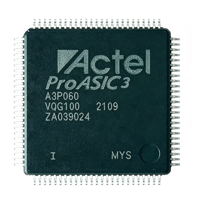
A3P060-2TQG144
A3P060-2TQG144 - ProASIC3 FPGA, 60K Gates | Microchip
The Microchip Technology A3P060-2TQG144 is a ProASIC3 field-programmable gate array (FPGA) with 60,000 system gates, 1,536 logic elements (equivalent to 700 LEs per Mouser), and 91 user I/Os, housed in a 144-pin LQFP (TQFP) package. It operates from a 1.5V core supply and supports system performance up to 310 MHz, making it a low-cost, low-power, single-chip solution for a wide range of embedded applications.
An FPGA (field-programmable gate array) is an integrated circuit that can be configured by the customer after manufacturing to implement arbitrary digital logic functions. Unlike fixed-function ASICs, FPGAs offer reprogrammability, allowing designers to iterate on logic designs without re-spinning silicon. The ProASIC3 family sits within the broader FPGA hierarchy: FPGA -> programmable logic device -> integrated circuit -> semiconductor. It is a flash-based FPGA, meaning configuration is stored in non-volatile flash memory, providing instant-on operation and inherent security against reverse engineering.
Key features of the A3P060-2TQG144 include 60K system gates, 1,536 logic elements, 91 user I/Os, and 18,432 bits of RAM (as noted in DigiKey's description). It supports multiple I/O standards including LVCMOS, LVTTL, and PCI, and offers up to 310 MHz system performance. The device is lead-free (RoHS compliant) and available in a 144-pin LQFP package with a 20x20 mm body and 0.5 mm pitch. It also features low power consumption, with typical static power of 0.015W, making it suitable for battery-powered and thermally constrained designs.
Technically, the ProASIC3 architecture uses a flash-based switch matrix that eliminates the need for external configuration memory, unlike SRAM-based FPGAs. This provides instant-on capability, single-chip operation, and enhanced security. The device includes dedicated phase-locked loops (PLLs) for clock management, and supports JTAG (IEEE 1149.1) for programming and boundary-scan testing. The 130nm process technology balances cost and performance, delivering 310 MHz performance while maintaining low power.
Typical applications include industrial control, automotive electronics, consumer devices, and communications infrastructure. For example, it can be used for motor control, sensor interfacing, protocol bridging, and display control. Its low power and small footprint make it ideal for portable and embedded systems where board space and battery life are critical.
When designing with the A3P060-2TQG144, ensure proper decoupling of the 1.5V core supply and 3.3V I/O supply with 0.1uF and 10uF capacitors placed close to the power pins. The device supports multiple I/O banks with independent supply voltages, so plan the power distribution carefully to meet I/O standard requirements. Also, use the JTAG interface for programming and consider using the on-chip PLLs for clock generation to reduce external component count.
This page synthesizes distributor pricing, drop-in alternatives, and practical design notes not found in the manufacturer datasheet, providing a comprehensive resource for engineers evaluating the A3P060-2TQG144 for their designs.
견적 요청
문의하기