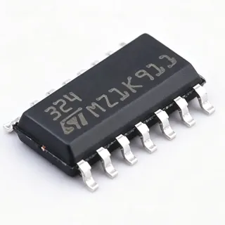
AD647SH/883B - Dual JFET Op Amp, 250uV, 1MHz | Analog Devices
MPN: AD647SH/883B ✓ Active| Qty | Unit Price | Extended |
|---|---|---|
| 1 | $22.19 | $22.19 |
| 10 | $20.5 | $205.00 |
| 100 | $18.8 | $1,880.00 |
| 500 | $17.1 | $8,550.00 |
| 1,000 | $15.4 | $15,400.00 |
AD647SH/883B Overview
An operational amplifier (op amp) is a high-gain voltage amplifier with differential inputs and a single-ended output. It is a fundamental building block in analog electronics, used in configurations such as inverting, non-inverting, differential, and instrumentation amplifiers. The JFET-input architecture provides very high input impedance and extremely low input bias current, making it ideal for interfacing with high-impedance sources such as sensors, photodiodes, and precision measurement circuits. The AD647SH/883B belongs to the family of precision op amps, which are characterized by low offset voltage, low noise, and low drift over temperature.
Key features of the AD647SH/883B include a maximum input offset voltage of 250 µV, a gain-bandwidth product of 1 MHz, and an input bias current of 35 pA. The device also offers a slew rate of and operates over a supply voltage range of . The dual-channel configuration saves board space and reduces component count in multi-channel systems. The TO-99 package provides a hermetic seal, protecting the die from moisture and contaminants, which is essential for military and aerospace applications.
The AD647SH/883B is built using Analog Devices' precision bipolar and JFET process technology, which combines the low offset and drift of bipolar transistors with the high input impedance of JFETs. This architecture achieves a typical input offset voltage drift of and a common-mode rejection ratio of . The device is fully specified over the military temperature range of -55°C to +125°C, making it suitable for defense and space systems.
Typical applications include precision data acquisition systems, medical instrumentation, test and measurement equipment, and active filters. The low input bias current allows direct connection to high-impedance sensors without significant loading errors. The dual-channel design is particularly useful for stereo audio processing and multi-channel industrial control loops.
When designing with the AD647SH/883B, ensure proper supply decoupling with 0.1 µF ceramic capacitors close to the supply pins. The TO-99 package requires careful handling to avoid damage to the leads. For high-impedance circuits, a guard ring around the input pins can reduce leakage currents and improve performance.
Drop-in alternatives for AD647SH/883B — same package, pin-to-pin compatible. Different-package parts requiring PCB rework are excluded.
Quick Comparison Tool — Select alternative parts for side-by-side comparison:
AD647SH
✅ Drop-In📋 Reference alternative (not in catalog)
AD644JH
✅ Drop-In📋 Reference alternative (not in catalog)
AD648TH
✅ Drop-In📋 Reference alternative (not in catalog)
OPA2111AM
✅ Drop-In ⚠️ Specs Unverified📋 Reference alternative (not in catalog)
AD647SH/883B Maximum Ratings & Electrical Characteristics
| Number of Channels | 2 |
| Input Offset Voltage (max) | 250 µV |
| Gain Bandwidth Product | 1 MHz |
| Input Bias Current (max) | 35 pA |
| Operating Temperature Range | -55°C to +125°C |
| Package | TO-99 (Metal Can) |
| Mounting Type | Through Hole |
| Amplifier Type | JFET Input |
| RoHS Status | unknown |
| Military Grade | Yes (883B suffix) |
AD647SH/883B Pin Configuration
| Pin 1 | OUT A — Output of amplifier A |
| Pin 2 | -IN A — Inverting input of amplifier A |
| Pin 3 | +IN A — Non-inverting input of amplifier A |
| Pin 4 | V- — Negative supply voltage |
| Pin 5 | +IN B — Non-inverting input of amplifier B |
| Pin 6 | -IN B — Inverting input of amplifier B |
| Pin 7 | OUT B — Output of amplifier B |
| Pin 8 | V+ — Positive supply voltage |
Typical Applications
AD647SH/883B is suitable for 6 applications: Precision Data Acquisition, Medical Instrumentation, Test and Measurement, Active Filters, Aerospace and Defense, Industrial Process Control.
Precision Data Acquisition
The AD647SH/883B's low offset voltage (250 µV) and low input bias current (35 pA) make it ideal for precision data acquisition systems. It can buffer high-impedance sensors without introducing significant errors, ensuring accurate signal conversion. The dual-channel configuration allows simultaneous sampling of multiple channels, reducing component count and board space. Its military temperature range ensures reliable operation in harsh environments.
Recommended
Medical Instrumentation
In medical instrumentation, the AD647SH/883B provides the low noise and low drift required for accurate biopotential measurements. Its high input impedance minimizes loading on electrodes, and the dual-channel design supports multi-lead ECG or EEG systems. The hermetic TO-99 package ensures long-term reliability in medical devices. The device's low bias current is particularly beneficial for high-impedance sensors used in diagnostic equipment.
Recommended
Test and Measurement
The AD647SH/883B is well-suited for test and measurement equipment such as digital multimeters and oscilloscope front-ends. Its low offset voltage and drift ensure accurate DC measurements, while the JFET input provides high input impedance to avoid loading the circuit under test. The dual-channel configuration is useful for differential measurements. The military temperature range allows use in field-deployed test equipment.
Recommended
Active Filters
The AD647SH/883B can be used in active filter designs, such as low-pass, high-pass, and band-pass filters, due to its 1 MHz gain-bandwidth product. The low input bias current allows the use of high-value resistors without introducing offset errors. The dual-channel package enables compact filter designs for stereo audio or multi-channel signal processing. Its low noise and drift ensure stable filter characteristics over temperature.
Recommended
Aerospace and Defense
The AD647SH/883B is designed for military and aerospace applications, as indicated by the 883B suffix. It operates over the full military temperature range and is available in a hermetic TO-99 package, providing resistance to moisture and contaminants. Its low drift and high reliability make it suitable for guidance systems, radar signal processing, and flight control electronics. The dual-channel design reduces weight and space in avionics.
Recommended
Industrial Process Control
In industrial process control, the AD647SH/883B provides accurate signal conditioning for sensors such as thermocouples, RTDs, and strain gauges. Its low offset voltage and drift ensure precise measurement over time, while the JFET input minimizes loading on high-impedance sensors. The dual-channel configuration allows monitoring of multiple process variables. The device's wide temperature range makes it suitable for harsh industrial environments.
Recommended
Recommended Products Summary
Engineering reference data for AD647SH/883B — comparison, design guidance, and compliance information.
Selection Guide
Comparison with Alternatives
| Parameter | This Product | AD647SH | AD644JH | AD648TH | OPA2111AM |
|---|---|---|---|---|---|
| Package | TO-99 | TO-99 | TO-99 | TO-99 | TO-99 |
| Brand | Analog Devices | Analog Devices | Analog Devices | Analog Devices | Texas Instruments |
| Number of Channels | 2 | 2 | 2 | 2 | 2 |
| Military Grade | Yes (883B) | No | No | No | No |
Key Differentiators
- Military-grade screening (883B suffix) (vs AD647SH)
- Ultralow input offset voltage (250 µV max) (vs AD648TH)
- Hermetic TO-99 package (vs OPA2111AM)
Design Notes
Ensure proper power supply decoupling. Place 0.1 µF ceramic capacitors as close as possible to the V+ and V- pins (pins 8 and 4) to filter high-frequency noise. Additionally, use 10 µF tantalum capacitors in parallel for low-frequency stability. The AD647SH/883B operates from dual supplies; verify the supply voltage range from the datasheet to avoid exceeding absolute maximum ratings.
For high-impedance inputs, use guard rings around the input pins (pins 2, 3, 5, 6) to minimize leakage currents. Keep traces short and shield them from noise sources. The TO-99 package has a metal can that can be connected to ground to provide shielding. Ensure proper soldering techniques to avoid thermal damage to the hermetic seal.
Do not exceed the absolute maximum supply voltage, as this can damage the device. The input bias current is extremely low (35 pA), so any contamination on the PCB can cause leakage currents that degrade performance. Use clean board handling and conformal coating if necessary. Also, note that the AD647SH/883B is a military-grade part; ensure proper ESD handling during assembly.
Compliance Information
Military-grade component may be exempt from RoHS. Compliance data not available from provided sources.