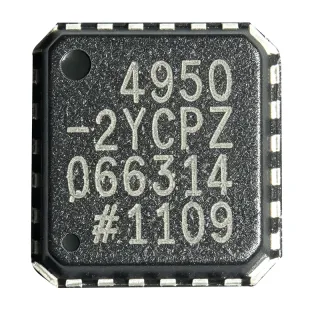
ADA4950-2YCPZ-RL7 - Selectable Gain Diff ADC Driver | Analog Devices
MPN: ADA4950-2YCPZ-RL7 ✓ Active| Qty | Unit Price | Extended |
|---|---|---|
| 1 | $12.05 | $12.05 |
| 10 | $10.85 | $108.50 |
| 100 | $9.64 | $964.00 |
| 500 | $8.43 | $4,215.00 |
| 1,000 | $7.22 | $7,220.00 |
ADA4950-2YCPZ-RL7 Overview
A differential ADC driver is a specialized amplifier that converts a single-ended or differential input signal into a balanced differential output, optimized to interface with the differential inputs of high-speed ADCs. It provides the necessary gain, common-mode voltage shifting, and low output impedance to drive the ADC's sampling capacitor without degrading signal integrity. In the signal chain hierarchy, a differential ADC driver sits between the sensor/amplifier stage and the ADC, ensuring that the ADC receives a clean, well-conditioned signal for accurate conversion.
Key features of the ADA4950-2 include a wide -3 dB bandwidth of 750 MHz, a slew rate of 2900 V/µs, and a low input voltage noise of 2.2 nV/√Hz. The device also offers a low offset voltage of 200 µV and a high output current of 60 mA, enabling it to drive the capacitive loads of ADCs effectively. The selectable gain feature simplifies design by eliminating the need for external resistor networks, reducing board space and component count.
Fabricated using Analog Devices' proprietary silicon-germanium (SiGe) complementary bipolar process, the ADA4950-2 achieves low distortion and noise at low power consumption. The device features a power-down mode that reduces quiescent current to 0.5 mA, making it suitable for power-sensitive applications. Its excellent dynamic performance, including a spurious-free dynamic range (SFDR) of -90 dBc at 10 MHz, ensures high-fidelity signal processing.
Typical applications include driving high-speed ADCs in communications, instrumentation, and medical imaging systems. It is also used in single-ended-to-differential conversion for balanced audio and video signals, and in differential signal conditioning for industrial sensors. The ADA4950-2's low power and small footprint make it ideal for portable and battery-powered equipment.
When designing with this device, ensure proper power supply decoupling with 0.1 µF and 10 µF capacitors placed close to the VCC and VEE pins. The output common-mode voltage can be set via the VOCM pin, which should be driven by a low-impedance source to maintain accuracy. For optimal performance, keep the feedback and gain paths short and use ground planes to minimize parasitic inductance.
Drop-in alternatives for ADA4950-2YCPZ-RL7 — same package, pin-to-pin compatible. Different-package parts requiring PCB rework are excluded.
Quick Comparison Tool — Select alternative parts for side-by-side comparison:
ADA4950-2YCPZ-R7
✅ Drop-In📋 Reference alternative (not in catalog)
ADA4950-2YCPZ-RL
✅ Drop-In📋 Reference alternative (not in catalog)
ADA4950-1YCPZ-R7
✅ Drop-In ⚠️ Specs Unverified📋 Reference alternative (not in catalog)
ADA4932-2YCPZ-R7
✅ Drop-In ⚠️ Specs Unverified📋 Reference alternative (not in catalog)
ADA4950-2YCPZ-RL7 Maximum Ratings & Electrical Characteristics
| Number of Channels | 2 |
| Gain Options | 1, 2, 3 (selectable) |
| Bandwidth (-3 dB) | 750 MHz |
| Slew Rate | 2900 V/µs |
| Input Voltage Noise | 2.2 nV/√Hz |
| Offset Voltage | 200 µV |
| Output Current | 60 mA |
| Supply Voltage Range (Single) | 3.3 V to 11 V |
| Supply Voltage Range (Dual) | ±1.65 V to ±5.5 V |
| Quiescent Current (per amp) | 9.5 mA |
| Power-Down Current | 0.5 mA |
| SFDR at 10 MHz | -90 dBc |
| Package | 24-Lead LFCSP (4x4 mm) |
| Operating Temperature Range | -40°C to +105°C |
| RoHS Status | Compliant |
ADA4950-2YCPZ-RL7 Pin Configuration
| Pin 1 | VOCM — Output common-mode voltage set |
| Pin 2 | PD — Power-down (active high) |
| Pin 3 | VEE — Negative supply (or ground) |
| Pin 4 | IN- — Inverting input |
| Pin 5 | IN+ — Non-inverting input |
| Pin 6 | VCC — Positive supply |
| Pin 7 | OUT+ — Non-inverting output |
| Pin 8 | OUT- — Inverting output |
| Pin 9 | G1 — Gain select 1 |
| Pin 10 | G0 — Gain select 0 |
| Pin 11 | VEE — Negative supply (or ground) |
| Pin 12 | IN- — Inverting input (channel 2) |
Typical Applications
ADA4950-2YCPZ-RL7 is suitable for 6 applications: High-Speed ADC Driver, Single-Ended to Differential Conversion, Communications Receivers, Medical Imaging Systems, Industrial Sensor Conditioning, Test and Measurement Equipment.
High-Speed ADC Driver
The ADA4950-2YCPZ-RL7 is ideal for driving high-speed ADCs in communications and instrumentation. Its 750 MHz bandwidth and low noise ensure that the ADC receives a clean, undistorted signal. The selectable gain of 1, 2, or 3 allows optimization of the signal level to match the ADC's full-scale range, improving dynamic range. The high output current of 60 mA can drive the ADC's sampling capacitor without slew-rate limitations, maintaining signal integrity at high frequencies.
Recommended
Single-Ended to Differential Conversion
The ADA4950-2YCPZ-RL7 converts single-ended signals to balanced differential outputs, which is essential for driving differential ADCs and reducing common-mode noise. Its low offset voltage of 200 µV and low noise of 2.2 nV/√Hz preserve signal accuracy. The device's common-mode voltage can be set via the VOCM pin, allowing interface with various ADC input ranges. This makes it suitable for sensor interfaces and data acquisition systems where signal fidelity is critical.
Recommended
Communications Receivers
In communications receivers, the ADA4950-2YCPZ-RL7 drives ADCs in IF or baseband stages. Its high SFDR of -90 dBc at 10 MHz ensures low distortion, preserving signal quality in dense spectral environments. The low power consumption of 19 mA is beneficial for multi-channel receivers. The selectable gain allows adjustment for varying signal strengths, improving receiver sensitivity and dynamic range.
Recommended
Medical Imaging Systems
The ADA4950-2YCPZ-RL7 is used in medical imaging systems such as ultrasound and MRI to drive ADCs that digitize analog signals from sensors. Its low noise and high bandwidth ensure accurate representation of fast-moving signals. The small 4x4 mm LFCSP package is ideal for space-constrained imaging probes. The device's low power consumption helps manage heat in sensitive medical equipment.
Recommended
Industrial Sensor Conditioning
The ADA4950-2YCPZ-RL7 conditions differential signals from industrial sensors such as strain gauges and accelerometers. Its selectable gain allows amplification of small sensor outputs to levels suitable for ADC conversion. The wide supply range of 3.3V to 11V accommodates various industrial power rails. The device's robust performance over -40°C to +105°C makes it suitable for harsh environments.
Recommended
Test and Measurement Equipment
In test and measurement equipment, the ADA4950-2YCPZ-RL7 drives ADCs in oscilloscopes, spectrum analyzers, and data loggers. Its high bandwidth and low distortion ensure accurate capture of high-frequency signals. The selectable gain provides flexibility in scaling input signals to match ADC ranges. The device's low power consumption is advantageous for portable test instruments.
Recommended
Recommended Products Summary
Engineering reference data for ADA4950-2YCPZ-RL7 — comparison, design guidance, and compliance information.
Selection Guide
Comparison with Alternatives
| Parameter | This Product | ADA4950-2YCPZ-R7 | ADA4950-2YCPZ-RL | ADA4950-1YCPZ-R7 | ADA4932-2YCPZ-R7 |
|---|---|---|---|---|---|
| Package | 24-Lead LFCSP (4x4 mm) | 24-Lead LFCSP (4x4 mm) | 24-Lead LFCSP (4x4 mm) | 24-Lead LFCSP (4x4 mm) | 24-Lead LFCSP (4x4 mm) |
| Brand | Analog Devices | Analog Devices | Analog Devices | Analog Devices | Analog Devices |
| Number of Channels | 2 | 2 | 2 | 1 | 2 |
| Gain Options | 1, 2, 3 (selectable) | 1, 2, 3 (selectable) | 1, 2, 3 (selectable) | 1, 2, 3 (selectable) | External resistors |
| Bandwidth (-3 dB) | 750 MHz | 750 MHz | 750 MHz | 750 MHz | 750 MHz |
| Slew Rate | 2900 V/µs | 2900 V/µs | 2900 V/µs | 2900 V/µs | 2900 V/µs |
| Input Voltage Noise | 2.2 nV/√Hz | 2.2 nV/√Hz | 2.2 nV/√Hz | 2.2 nV/√Hz | 2.2 nV/√Hz |
| Supply Voltage Range | 3.3V to 11V (single) | 3.3V to 11V (single) | 3.3V to 11V (single) | 3.3V to 11V (single) | 3.3V to 11V (single) |
Key Differentiators
- Selectable gain without external resistors (vs ADA4932-2YCPZ-R7)
- Lower power consumption (vs THS4509RGT)
- Higher bandwidth (vs ADA4932-2YCPZ-R7)
Design Notes
Ensure proper power supply decoupling. Place 0.1 µF and 10 µF capacitors as close as possible to the VCC and VEE pins. The 10 µF capacitor provides bulk decoupling for low-frequency transients, while the 0.1 µF handles high-frequency noise. Use a low-inductance ground plane to minimize parasitic effects.
For optimal performance, keep the feedback and gain paths short and direct. The selectable gain pins (G0, G1) should be tied to VCC or GND with short traces to avoid parasitic inductance. Use a solid ground plane under the device to reduce noise coupling. The exposed pad should be soldered to the ground plane for thermal and electrical performance.
Do not leave the power-down (PD) pin floating; tie it to GND for normal operation. The VOCM pin must be driven by a low-impedance source to set the output common-mode voltage accurately. Avoid exceeding the absolute maximum supply voltage of 12V, as this can damage the device. Also, ensure the gain select pins are set correctly to avoid unintended gain settings.
Compliance Information
RoHS compliant per distributor listings. No AEC-Q100 qualification indicated for this part.