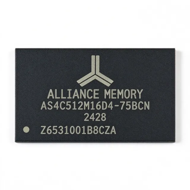
AS4C512M16D4-75BCN - 8Gb DDR4 SDRAM 2666MT/s | Alliance Memory
MPN: AS4C512M16D4-75BCN ✓ Active| Qty | Unit Price | Extended |
|---|---|---|
| 1 | $10.11 | $10.11 |
| 10 | $9.6 | $96.00 |
| 100 | $8.9 | $890.00 |
| 500 | $8.3 | $4,150.00 |
| 1,000 | $7.75 | $7,750.00 |
AS4C512M16D4-75BCN Overview
DDR4 SDRAM (Double Data Rate 4 Synchronous Dynamic Random-Access Memory) is the fourth generation of high-bandwidth volatile memory. It transfers data on both edges of the clock, uses an 8n-prefetch architecture to achieve high throughput, and operates at a lower 1.2V core supply than DDR3's 1.5V, reducing dynamic power. Within the memory hierarchy it sits at the DRAM level of the semiconductor memory family (SDRAM -> DDR4 SDRAM -> memory IC), serving as the main working memory in embedded, industrial, and networking systems.
Key features include the 8Gb density in a wide x16 organization, a commercial temperature range of 0C to +95C, sixteen internal banks, programmable CAS latency, on-die termination (ODT) for signal integrity, and auto-refresh/self-refresh power-saving modes. Alliance Memory positions this family as a reliable drop-in, pin-for-pin-compatible replacement for numerous similar solutions, eliminating costly redesigns and part requalification.
Technically, the 8n prefetch reads or writes an 8n-bit internal burst from the DRAM core and delivers eight n-bit transfers per half clock at the I/O pins. Bank group addressing, burst length control, and calibrated output drive support stable 2666 MT/s operation on standard memory controllers.
Typical applications include embedded computing and industrial PC main memory, networking processor line cards, test equipment, and graphics/display systems that need a wide 16-bit data bus with 8Gb capacity.
When designing with this device, place decoupling capacitors on every VDD/VDDQ ball pair, keep the 1.2V rail within tolerance, and follow the datasheet FBGA routing guidelines for length-matched address/command lines.
This page synthesizes distributor pricing, drop-in alternatives, and practical design notes not found in the manufacturer datasheet.
Drop-in alternatives for AS4C512M16D4-75BCN — same package, pin-to-pin compatible. Different-package parts requiring PCB rework are excluded.
Variants in this series
Same-series models that are drop-in compatible with AS4C512M16D4-75BCN (same form factor and footprint) — differing in Data Rate, Mounting Type, Operating Temperature Range, Package, Refresh Modes.
Quick Comparison Tool — Select alternative parts for side-by-side comparison:
AS4C512M16D4-75BIN
✓ In Stock
$8.99 / Unit
View Datasheet →AS4C512M16D4A-62BCN
✓ In Stock
$7.2 / Unit
View Datasheet →AS4C512M16D4B-62BCNTR
✓ In Stock
$8.1 / Unit
View Datasheet →MT40A512M16HA-083E
✓ In Stock
Contact for price
View Datasheet →K4A8G165WC-BCPB
✓ In Stock
$1.31 / Unit
View Datasheet →K4A8G165WB-BCWE
✓ In Stock
$6.55 / Unit
View Datasheet →MT40A512M16LY-075E
📋 Reference alternative (not in catalog)
AS4C512M16D4-75BCN Maximum Ratings & Electrical Characteristics
| Memory Type | DDR4 SDRAM |
| Density | 8 Gbit |
| Organization | 512M x 16 |
| Data Rate | 2666 MT/s (DDR4-2666) |
| Clock Frequency | 1.333 GHz |
| Supply Voltage | 1.2 V |
| CAS Latency | 18 |
| Access Time | 18 ns |
| Number of Banks | 16 |
| Prefetch Architecture | 8n |
| Interface | Parallel |
| Package | 96-FBGA (7.5 mm x 13 mm) |
| Operating Temperature Range | 0C to +95C (Commercial) |
| Mounting Type | Surface Mount (FBGA) |
| Packaging | Tray |
| Refresh Modes | Auto-refresh, Self-refresh |
| On-Die Termination | Yes (ODT) |
AS4C512M16D4-75BCN 96-fbga (7.5 mm x 13 mm) Pin Configuration Guide
Pin configuration for AS4C512M16D4-75BCN (96-fbga (7.5 mm x 13 mm) package). This digital IC includes GPIO, communication interfaces (UART, SPI, I2C), and power pins. Refer to the manufacturer datasheet for alternate pin functions and configuration options. Essential for embedded system design and PCB layout.

No detailed pinout data available for AS4C512M16D4-75BCN.
Refer to the datasheet for full pin configuration.
Typical Applications
AS4C512M16D4-75BCN is suitable for 6 applications: Embedded Computing Main Memory, Networking Equipment Line Cards, Industrial PC and HMI Systems, Test and Measurement Instruments, Graphics and Display Frame Buffers, Server and Storage Controller Memory.
Embedded Computing Main Memory
The AS4C512M16D4-75BCN serves as main system memory for embedded x86 and ARM compute modules, where its 8Gb density organized 512M x 16 provides 1 GB per device and the wide 16-bit bus simplifies 32-bit and 64-bit interleaved layouts. Running DDR4-2666 at CL18 on a 1.2V rail, it delivers 21.3 GB/s per device at lower dynamic power than comparable DDR3 solutions. Placed on the memory controller's length-matched fly-by address/command bus with on-die termination engaged, it supports stable operation with standard SO-DIMM-style routing; Alliance's positioning as a pin-for-pin drop-in replacement protects long-life embedded designs from vendor EOL.
Recommended
Networking Equipment Line Cards
Network processors and switch ASICs require deep packet buffers with high sustained bandwidth, making the AS4C512M16D4-75BCN's 8Gb capacity and 2666 MT/s x16 interface well suited to buffering and queue-management memory. The sixteen-bank organization allows multiple open rows to hide core latency during bursty traffic, while the 8n prefetch keeps sequential throughput at 21.3 GB/s per device from a single 1.2V supply - critical in systems where line-card power budgets are tightly enforced. Auto-refresh and self-refresh modes allow buffer retention during low-traffic periods. Vendor second-sourcing across the JEDEC-compatible alternatives mitigates long-term supply risk for multi-year networking programs.
Recommended
Industrial PC and HMI Systems
Industrial PCs, vision controllers, and HMIs benefit from the AS4C512M16D4-75BCN's combination of density and supply-chain longevity. The 512M x 16 organization allows one or two devices to populate a 16/32-bit memory channel, reducing BOM count versus stacked smaller parts, while the 1.2V DDR4 rail keeps total memory power low inside fanless enclosures. Note the commercial 0C to +95C rating: for unheated factory-floor enclosures, substitute the pin-identical AS4C512M16D4-75BIN industrial-grade part without PCB change. Alliance Memory's long-life DRAM roadmap and drop-in compatibility policy specifically target industrial customers needing multi-year continuity.
Recommended
Test and Measurement Instruments
Oscilloscopes, logic analyzers, and signal generators need deep acquisition memory with deterministic burst performance. The AS4C512M16D4-75BCN's 8Gb capacity supports long waveform captures, and its CL18 DDR4-2666 interface with programmable burst length lets instrument FPGAs sustain streaming writes during trigger events. On-die termination simplifies multi-drop point-to-point routing between the FPGA memory controller and the DRAM. Because Alliance Memory provides pin-for-pin-compatible replacements within the family, instrument vendors can qualify one PCB footprint across speed grades (-75, -62) and temperature grades (CN/IN) to segment product lines without respins.
Recommended
Graphics and Display Frame Buffers
Display and lightweight graphics subsystems use the AS4C512M16D4-75BCN as frame-buffer memory where its wide 16-bit data bus matches typical LCD/DP interface bandwidth requirements. At 2666 MT/s the device sustains the multi-hundred-MB/s streams needed for multi-panel 1080p or single 4K refresh with headroom for 2D acceleration overlays. The 1.2V supply and self-refresh mode support low-power idle states in display-sleep scenarios. Designers should budget refresh overhead (per JEDEC DDR4 timing) when calculating guaranteed frame-buffer write bandwidth and place ODT settings per the controller's signal-integrity sweep at 2666 MT/s.
Recommended
Server and Storage Controller Memory
RAID controllers, storage appliances, and edge servers use discrete DDR4 devices for write-cache and metadata memory. The AS4C512M16D4-75BCN's 8Gb per device lets a 64-bit channel reach 4 GB with four parts, and its 2666 MT/s rate supplies the bandwidth that cache-flush transactions demand. Battery/supercap-backed designs exploit self-refresh to hold cache contents through power events. Alliance Memory's drop-in, pin-for-pin compatibility with mainstream DDR4 solutions means storage OEMs can dual-source this footprint against Samsung K4A8G165 and Micron MT40A512M16 parts, protecting against allocation cycles that historically affect DRAM supply during demand spikes.
Recommended
Recommended Products Summary
Engineering reference data for AS4C512M16D4-75BCN — comparison, design guidance, and compliance information.
Selection Guide
Comparison with Alternatives
| Parameter | This Product | AS4C512M16D4-75BIN | MT40A512M16LY-075E | K4A8G165WC-BCPB | MT40A512M16HA-083E |
|---|---|---|---|---|---|
| Package | 96-FBGA (7.5x13mm) | 96-FBGA (7.5x13mm) - same | 96-FBGA (7.5x13mm) - same | 96-FBGA (7.5x13mm) - same | 96-FBGA (7.5x13mm) - same |
| Brand | Alliance Memory | Alliance Memory | Micron Technology | Samsung Electronics | Micron Technology |
| Density | 8 Gbit | 8 Gbit | 8 Gbit | 8 Gbit | 8 Gbit |
| Organization | 512M x 16 | 512M x 16 | 512M x 16 | 512M x 16 | 512M x 16 |
| Data Rate | 2666 MT/s | 2666 MT/s | 2666 MT/s | 2666 MT/s | 2400 MT/s (-11%) |
| Supply Voltage | 1.2 V | 1.2 V | 1.2 V | 1.2 V | 1.2 V |
| CAS Latency | CL18 | CL18 | CL18 | CL19 | CL17 |
Key Differentiators
- Lowest CAS latency at DDR4-2666 in this comparison set (vs K4A8G165WC-BCPB)
- Guaranteed drop-in replacement strategy for long-life designs (vs MT40A512M16LY-075E)
- Single-source footprint covering both temperature and speed grades (vs AS4C512M16D4-75BIN / AS4C512M16D4A-62BCN)
Design Notes
Provide a single 1.2V rail for both VDD and VDDQ with dedicated decoupling: place at least one 0.1uF ceramic within 2mm of each supply ball pair plus bulk capacitance (e.g., 47-100uF) per device. Keep the rail within JEDEC DDR4 tolerance (nominal +/-5%). Because this is a 2666 MT/s device, simultaneous switching currents on the 16 DQ lines create supply droop; a local plane pair under the FBGA keeps the power delivery network impedance low. Verify peak current against the datasheet IDD specifications for your read/write duty cycle before sizing the VRM.
Route the DDR4 address/command/control bus in a fly-by topology with length-matched segments per the Alliance Memory 8Gb DDR4 datasheet routing guidelines; keep DQ/DQS/DM groups length-matched within +/-25 mils (typical for 2666 MT/s) and reference them to a continuous ground plane. Avoid routing under the FBGA ball field. Termination is handled by on-die termination (ODT), so set controller ODT values during read/write training rather than adding external bus termination resistors. Maintain impedance control at 40 ohms for the clock/strobe nets per standard DDR4 PCB stackups.
Two frequent mistakes with this device: (1) using the -75BCN commercial grade in enclosures that can exceed +95C - switch to the pin-identical AS4C512M16D4-75BIN industrial grade instead of redesigning; (2) reusing a controller memory-training table from another DRAM vendor without re-running read/write leveling - even JEDEC-compatible parts differ in register defaults (e.g., CL19 vs CL18 on Samsung K4A8G165WC). Always re-run training after any vendor change, and verify refresh interval settings for the commercial temperature range before closing the design.
Compliance Information
Compliance status not stated in the provided verified data; modern DDR4 SDRAM is typically RoHS-compliant but confirm against the Alliance Memory datasheet and product page before export documentation.

