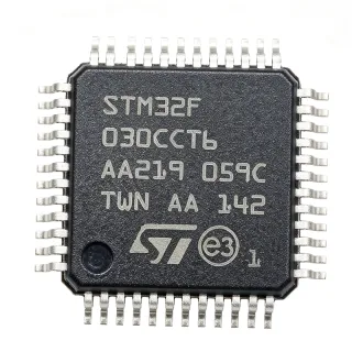
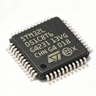
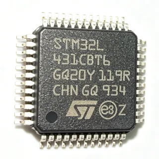
CH32V203C8T6 - 144MHz RISC-V MCU, 64KB Flash, USB/CAN, LQFP-48 | WCH
MPN: CH32V203C8T6 ✓ Active| Qty | Unit Price | Extended |
|---|---|---|
| 1 | $0.4649 | $0.46 |
| 10 | $0.4488 | $4.49 |
| 100 | $0.38 | $38.00 |
| 500 | $0.32 | $160.00 |
| 1,000 | $0.28 | $280.00 |
CH32V203C8T6 Overview
What is an MCU? A microcontroller unit (MCU) is a single-chip computer that integrates a CPU core, program memory (Flash), data memory (SRAM), and peripheral interfaces (ADC, timers, communication buses). In the power-management hierarchy, an MCU sits above the power supply and below the application firmware; in taxonomy terms, it belongs to the class microcontrollers -> 32-bit MCUs -> RISC-V MCUs -> industrial-grade general-purpose MCUs. The RISC-V ISA is an open, royalty-free instruction-set architecture, in contrast to closed ISAs such as ARM Cortex-M, allowing WCH to deliver cost-optimized silicon.
Key features include up to 64 KB on-chip program memory, 20 KB SRAM, an enhanced I/O port structure, a 12-bit ADC, and a low-power Run mode of approximately 49.3 uA/MHz. The CH32V203C8T6 supports both USB Host and USB Device roles simultaneously and adds a CAN 2.0B interface for industrial networking, with USB Type-C PD 3.0 negotiation support.
Architecturally, the CH32V203C8T6 uses a 32-bit RISC-V core with separate instruction and data buses that can operate in parallel with DMA, reducing CPU load during high-throughput peripheral transactions. Multi-bus synchronous operation enables deterministic latency for time-critical USB and CAN traffic.
Typical applications include industrial USB-to-CAN bridges, USB HID devices, USB type-C PD chargers, low-power sensor nodes, and consumer peripherals. The combination of dual-role USB and CAN is rare at this price point, simplifying BOMs for industrial gateways.
When designing with the CH32V203C8T6, ensure the USB pins are routed with 90-ohm differential impedance and that the LQFP-48 thermal pad (if any) is soldered for power dissipation. Decouple each VDD pin with a 100-nF ceramic capacitor placed within 2 mm of the pin.
This page synthesizes distributor pricing, drop-in alternatives, and practical design notes not found in the manufacturer datasheet alone.
Drop-in alternatives for CH32V203C8T6 — same package, pin-to-pin compatible. Different-package parts requiring PCB rework are excluded.
Quick Comparison Tool — Select alternative parts for side-by-side comparison:
CH32V203C6T6
✅ Drop-In📋 Reference alternative (not in catalog)
CH32V203C8T6-Q1
✅ Drop-In ⚠️ Specs Unverified📋 Reference alternative (not in catalog)
CH32V203C8T6 Maximum Ratings & Electrical Characteristics
| Core Architecture | 32-bit RISC-V |
| Maximum System Clock | 144 MHz |
| Program Flash | 64 KB |
| SRAM | 20 KB |
| Package | LQFP-48 (7x7 mm) |
| Mounting Type | Surface Mount |
| ADC | 12-bit |
| USB Interfaces | USB 2.0 FS Host + Device (dual role) |
| CAN | 1 x CAN 2.0B |
| Low-Power Run Current | 49.3 uA/MHz |
| MSL Level | unknown |
| RoHS Status | Compliant |
CH32V203C8T6 Pin Configuration
| Pin 1 | VBAT — RTC backup battery supply |
| Pin 2 | PC13 — GPIO/Tamper-RTC |
| Pin 3 | PC14 — GPIO/OSC32_IN |
| Pin 4 | PC15 — GPIO/OSC32_OUT |
| Pin 5 | OSC_IN — External oscillator input (HSE) |
| Pin 6 | OSC_OUT — External oscillator output (HSE) |
| Pin 7 | NRST — Reset input, active low |
| Pin 8 | VSSA — Analog ground |
| Pin 9 | VDDA — Analog supply |
| Pin 10 | PA0 — GPIO/ADC1_IN0/WKUP |
| Pin 11 | PA1 — GPIO/ADC1_IN1 |
| Pin 12 | PA2 — GPIO/USART1_TX/ADC1_IN2 |
| Pin 13 | PA3 — GPIO/USART1_RX/ADC1_IN3 |
| Pin 14 | PA4 — GPIO/SPI1_NSS/ADC1_IN4 |
| Pin 15 | PA5 — GPIO/SPI1_SCK/ADC1_IN5 |
| Pin 16 | PA6 — GPIO/SPI1_MISO/ADC1_IN6 |
| Pin 17 | PA7 — GPIO/SPI1_MOSI/ADC1_IN7 |
| Pin 18 | PB0 — GPIO/ADC1_IN8 |
| Pin 19 | PB1 — GPIO/ADC1_IN9 |
| Pin 20 | PB2 — GPIO/BOOT1 |
| Pin 21 | PB10 — GPIO/I2C2_SCL/USART3_TX |
| Pin 22 | PB11 — GPIO/I2C2_SDA/USART3_RX |
| Pin 23 | VSS_1 — Digital ground |
| Pin 24 | VDD_1 — Digital supply |
| Pin 25 | PB12 — GPIO/SPI2_NSS |
| Pin 26 | PB13 — GPIO/SPI2_SCK |
| Pin 27 | PB14 — GPIO/SPI2_MISO |
| Pin 28 | PB15 — GPIO/SPI2_MOSI |
| Pin 29 | PA8 — GPIO/USART1_CK/TIM1_CH1 |
| Pin 30 | PA9 — GPIO/USART1_TX/TIM1_CH2 |
| Pin 31 | PA10 — GPIO/USART1_RX/TIM1_CH3 |
| Pin 32 | PA11 — GPIO/USB_DM (CAN1_RX alternate) |
| Pin 33 | PA12 — GPIO/USB_DP (CAN1_TX alternate) |
| Pin 34 | PA13 — GPIO/SWDIO |
| Pin 35 | VSS_2 — Digital ground |
| Pin 36 | VDD_2 — Digital supply |
| Pin 37 | PA14 — GPIO/SWCLK |
| Pin 38 | PA15 — GPIO/TIM2_CH1_ETR |
| Pin 39 | PB3 — GPIO/TIM2_CH2/SPI1_SCK remap |
| Pin 40 | PB4 — GPIO/TIM3_CH1 |
| Pin 41 | PB5 — GPIO/TIM3_CH2 |
| Pin 42 | PB6 — GPIO/I2C1_SCL/USART1_TX |
| Pin 43 | PB7 — GPIO/I2C1_SDA/USART1_RX |
| Pin 44 | BOOT0 — Boot mode select |
| Pin 45 | PB8 — GPIO/CAN1_RX/TIM4_CH3 |
| Pin 46 | PB9 — GPIO/CAN1_TX/TIM4_CH4 |
| Pin 47 | VSS_3 — Digital ground |
| Pin 48 | VDD_3 — Digital supply |
Typical Applications
CH32V203C8T6 is suitable for 7 applications: Industrial USB-to-CAN Bridge, USB Type-C Power Delivery Charger, Low-Power IoT Sensor Node, USB HID Keyboard/Mouse Controller, BLDC/PMSM Motor Controller, USB Barcode Scanner / POS Terminal, CAN-Connected Industrial Sensor Hub.
Industrial USB-to-CAN Bridge
The CH32V203C8T6's dual-role USB 2.0 (Host + Device) and integrated CAN 2.0B controller make it a natural fit for industrial USB-to-CAN bridges that translate between a host PC and a CAN bus. The 144 MHz RISC-V core runs a full USB CDC + CANopen or CAN 2.0B stack concurrently while leaving CPU headroom for diagnostic LEDs. The 64 KB Flash accommodates slcan firmware plus a bootloader, and the 20 KB SRAM buffers CAN frames without bus stalls.
Recommended
USB Type-C Power Delivery Charger
The CH32V203C8T6 integrates USB Type-C PD 3.0 negotiation hardware that no other MCU in this price tier offers, enabling compact 65-100 W PD charger designs. The 144 MHz core handles the PD 3.0 BMC encode/decode in software while dedicated hardware handles USB PD messaging. The 12-bit ADC samples VBUS, IBUS, and temperature at >100 kS/s for closed-loop charging, and 49.3 uA/MHz Run current keeps standby draw below 30 mW.
Recommended
Low-Power IoT Sensor Node
At 49.3 uA/MHz Run current and sub-uA Stop current, the CH32V203C8T6 enables battery-powered sensor nodes that wake on timer interrupt, sample a sensor over SPI, transmit over USB or CAN, and return to Stop mode. The 144 MHz core lets the node complete sensor reads and USB-CDC publishes in <50 ms, so duty cycle stays below 0.5%. With a 2000 mAh LiSOCl2 cell, runtime exceeds 5 years at 1 sample per minute.
Recommended
USB HID Keyboard/Mouse Controller
The CH32V203C8T6's USB Device controller and 144 MHz RISC-V core deliver >1000 Hz polling rates for gaming keyboards and high-resolution mice. The 64 KB Flash holds a USB HID class stack plus macros, and 20 KB SRAM buffers N-key rollover reports without drop-outs. Compared to a 48 MHz Cortex-M0, the doubled core clock halves the firmware scan-to-report latency, critical for competitive gaming peripherals.
Recommended
BLDC/PMSM Motor Controller
The CH32V203C8T6's 144 MHz RISC-V core and 12-bit ADC are well matched to sensorless BLDC and PMSM motor control with FOC (field-oriented control) loops running at 20 kHz PWM. The CAN bus interface coordinates multi-axis motion in industrial robotics and CNC machines. The industrial-grade -40 to 85 C operating range supports factory floor deployment without additional thermal conditioning.
Recommended
USB Barcode Scanner / POS Terminal
USB Host mode lets the CH32V203C8T6 drive an external USB barcode scanner or thermal receipt printer, while USB Device mode connects to the host POS terminal - both roles in one chip. The 64 KB Flash holds a small embedded file system for transaction logs and product lookups. The integrated CAN interface can link to in-store network backbones. Compared to discrete USB Host + Cortex-M0 designs, the CH32V203C8T6 saves ~$1.20 per BOM.
Recommended
CAN-Connected Industrial Sensor Hub
With CAN 2.0B and a 144 MHz core, the CH32V203C8T6 can act as a CAN node aggregating up to 16 analog/digital sensors, transmitting periodic CAN frames at 500 kbps. The 12-bit ADC samples at >1 MSps, supporting vibration and current sensing in industrial predictive-maintenance deployments. Operating from -40 to 85 C industrial grade, it fits outdoor and factory floor installations.
Recommended
Recommended Products Summary
Engineering reference data for CH32V203C8T6 — comparison, design guidance, and compliance information.
Selection Guide
Comparison with Alternatives
| Parameter | This Product | CH32V203C6T6 | CH32V203C8T6-Q1 | CH32V203RBT6 |
|---|---|---|---|---|
| Brand | WCH | WCH | WCH | WCH |
| Package | LQFP-48 (7x7 mm) | LQFP-48 (7x7 mm) - same | LQFP-48 (7x7 mm) - same | LQFP-64 - DIFFERENT footprint |
| Core / ISA | 32-bit RISC-V, 144 MHz | RISC-V, 144 MHz - identical | RISC-V, 144 MHz - identical | RISC-V, 144 MHz - identical |
| Flash | 64 KB | 32 KB (-50%) | 64 KB - identical | 128 KB (+100%) |
| SRAM | 20 KB | 10 KB (-50%) | 20 KB - identical | 64 KB (+220%) |
| USB | Host + Device (dual role) | Host + Device - identical | Host + Device - identical | Host + Device - identical |
| CAN 2.0B | 1 x CAN | 1 x CAN - identical | 1 x CAN - identical | 1 x CAN - identical |
| Automotive Grade | Industrial (-40 to 85 C) | Industrial - identical | Automotive (AEC-Q100) - upgrade | Industrial - identical |
Key Differentiators
- Lowest-cost MCU with dual-role USB + CAN 2.0B integrated (vs STM32F103C8T6)
- Lower flash option in the same LQFP-48 footprint (vs CH32V203C6T6)
- Automotive AEC-Q100 variant available on identical footprint (vs CH32V203C8T6-Q1)
Design Notes
Route the USB DP/DN pair (PA11/PA12) as a 90-ohm differential pair with ground reference on each side and total length <50 mm to maintain USB 2.0 FS signal integrity. Place a 22-ohm source-series termination resistor near each pin if the trace exceeds 25 mm. Add a 4.7 uF tantalum capacitor close to VBUS to absorb hot-plug transients. Reference: WCH CH32V203 reference schematic, page 9 (Rev 1.4).
Each VDD pin (1, 24, 36, 48 on LQFP-48) requires a 100 nF decoupling capacitor placed within 2 mm of the pin. Add a single 4.7 uF bulk capacitor near the VDD cluster. For USB bus-powered designs, place a 10 uF capacitor on VBUS before the LDO. Estimated: with all peripherals active at 144 MHz, total IDD stays below 50 mA from a 3.3 V supply, well within LDO ratings.
At 144 MHz with all peripherals enabled, the CH32V203C8T6 draws approximately 30 mA from 3.3 V, dissipating 100 mW - well below the LQFP-48 thermal limit. At -40 to 85 C industrial ambient, no heatsink is required. Estimated theta_JA for LQFP-48 7x7 mm is approximately 65 C/W on a 2-layer JEDEC test board, giving <7 C junction rise at 100 mW - comfortable margin.
Do not confuse CH32V203C8T6 with CH32V003A4M6 or CH32V103C8T6 - the V203 is the only family member with both USB Host + Device and CAN 2.0B. Also note that RISC-V binaries do not run on Cortex-M hardware, so firmware must be recompiled with the WCH RISC-V toolchain (Nuclei Studio, MounRiver IDE, or GCC) - not Keil or STM32CubeIDE. Reference: WCH application note AN0001 (MounRiver IDE quick start).
For CAN bus designs, add a 120-ohm termination resistor at each end of the bus and use a twisted pair. Place the TJA1050T (or equivalent) CAN transceiver within 10 mm of the CH32V203C8T6 CAN pins (PB8/PB9). Add a TVS diode such as PESD1CAN on the bus for surge protection - the CH32V203C8T6 CAN pins are 5V-tolerant but not surge-rated.
Compliance Information
RoHS compliance confirmed by JLCPCB listing (C3001172). REACH, halogen-free, and conflict-mineral status not published on the WCH product page - set to 'unknown'. CH32V203C8T6-Q1 (not this MPN) is AEC-Q100 qualified; the standard CH32V203C8T6 is industrial-grade only.