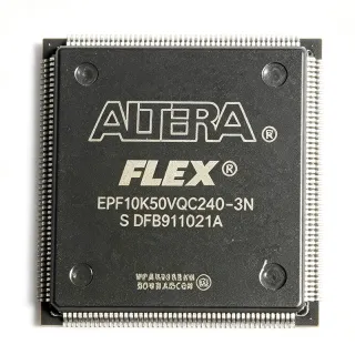
EP20K100EQC240-2X FPGA - APEX 20KE 183 I/O 240-QFP | Intel
MPN: EP20K100EQC240-2X ✗ End of Life| Qty | Unit Price | Extended |
|---|---|---|
| 1 | $58.75 | $58.75 |
| 10 | $53.1 | $531.00 |
| 100 | $48.2 | $4,820.00 |
| 500 | $44.5 | $22,250.00 |
| 1,000 | $39.8 | $39,800.00 |
EP20K100EQC240-2X Overview
An FPGA is a reconfigurable digital integrated circuit whose logic elements, routing resources, and I/O functions are programmed after manufacturing. FPGAs sit between fixed-function ASICs and software processors in the system hierarchy: they provide massive parallel custom hardware while remaining field-upgradable. The APEX-20KE family belongs to older Altera mid-density FPGAs and supports the PLD/CPLD and gate-array replacement role in legacy and industrial systems.
The EP20K100EQC240-2X offers 4,160 logic elements to implement control, data-path, and interfacing logic. Its 53,248 RAM bits allow small FIFOs, line buffers, or register files without external memory. With 183 user I/Os, it can connect to multiple parallel buses, ADC/DAC interfaces, and backplane signals. The 240-pin QFP package is easy to solder and inspect compared with fine-pitch BGA alternatives.
Technically, the APEX-20KE architecture combines look-up-table based logic, embedded memory, and a fast interconnect fabric. Fabricated on a 0.22 µm CMOS process, the FPGA integrates up to 100K typical system gates and supports vendor design flows. The -2X suffix denotes a specific speed/ordering grade; actual timing should be confirmed from the APEX 20K datasheet when targeting a frequency above 250 MHz.
The EP20K100EQC240-2X is commonly used in telecom line cards, industrial controllers, data acquisition systems, signal-conversion front-ends, and legacy FPGA sockets. Its 5.0 V-tolerant I/O simplifies direct connection to legacy 3.3 V or 5.0 V logic families. The 1.8 V core also helps reduce dynamic switching power compared with earlier 2.5 V or 3.3 V programmable devices.
Designers should verify the complete voltage and power-up requirements, including VCCINT and VCCIO rails, before layout. Because this is a legacy APEX device, users should confirm configuration-device compatibility and BSDL/model availability for boundary-scan testing in new board designs.
This page combines current distributor availability, verified package and I/O data, drop-in APEX-20K family alternatives, and practical design notes that are not all repeated in a single manufacturer datasheet view, giving engineers a faster component evaluation workflow.
Drop-in alternatives for EP20K100EQC240-2X — same package, pin-to-pin compatible. Different-package parts requiring PCB rework are excluded.
Variants in this series
Same-series models that are drop-in compatible with EP20K100EQC240-2X (same form factor and footprint) — differing in Package, Operating Temperature, Mounting Type, System Gates, User I/Os.
Quick Comparison Tool — Select alternative parts for side-by-side comparison:
EP20K100EQC240-1
✅ Drop-In📋 Reference alternative (not in catalog)
EP20K100EQC240-1N
✅ Drop-In📋 Reference alternative (not in catalog)
EP20K100EQC240-2
✅ Drop-In📋 Reference alternative (not in catalog)
EP20K100EQC240-2N
✅ Drop-In📋 Reference alternative (not in catalog)
EP20K100EQC240-3N
✅ Drop-In✓ In Stock
$51.84 / Unit
View Datasheet →EP20K100EQC240
✅ Drop-In📋 Reference alternative (not in catalog)
EP20K100EQC240-2X Maximum Ratings & Electrical Characteristics
| Device Family | APEX-20KE |
| Device Type | FPGA / Field Programmable Gate Array |
| Number of Logic Elements / Cells | 4160 |
| Typical Gate Count | 100K gates |
| Total RAM Bits | 53,248 bits |
| User I/Os | 183 |
| Pin Count | 240 |
| Package | 240-BFQFP / PQFP |
| Mounting Type | Surface Mount |
| Core Supply Voltage | 1.8 V |
| Maximum Internal Frequency | 250 MHz |
| Propagation Delay (tPD) | 1.6 ns |
| Operating Temperature Range | 0°C to +85°C |
| Process Technology | 0.22 µm CMOS |
| I/O Tolerance | 5.0-V tolerant |
| Lifecycle Note | Legacy APEX-20KE device; verify long-term availability |
EP20K100EQC240-2X 240-bfqfp / pqfp Pin Configuration Guide
Pin configuration for EP20K100EQC240-2X (240-bfqfp / pqfp package). This digital IC includes GPIO, communication interfaces (UART, SPI, I2C), and power pins. Refer to the manufacturer datasheet for alternate pin functions and configuration options. Essential for embedded system design and PCB layout.

No detailed pinout data available for EP20K100EQC240-2X.
Refer to the datasheet for full pin configuration.
Typical Applications
EP20K100EQC240-2X is suitable for 6 applications: Telecom & Networking Infrastructure, Industrial Control & Automation, Data Acquisition & Instrumentation, Digital Signal Processing Front-End, Legacy System Lifecycle Extension, Custom Logic and I/O Expansion.
Telecom & Networking Infrastructure
The EP20K100EQC240-2X is well suited for telecom line cards and networking equipment that need medium-density protocol bridging, parallel bus interface, and glue logic. Its 183 user I/Os allow connection to multiple UTOPIA, POS-PHY, or general-purpose bus segments, while its 4,160 logic elements handle framing state machines and FIFO control. The 5.0 V-tolerant I/O is an advantage when connecting to legacy 3.3 V or 5.0 V PHYs without adding level shifters. In a line-card design the FPGA sits between backplane transceivers and the host controller, offloading repetitive packet parsing and status generation from the CPU. Since the device is a 1.8 V-core part, use separate bulk and high-frequency decoupling on VCCINT and VCCIO. Legacy speed bins should be verified for the exact line rate; for new installations, confirm the configuration file supports the device variant before deployment.
Recommended
Industrial Control & Automation
Industrial controllers often need custom pulse-width modulation, quadrature encoder decoding, safety interlocks, and parallel field-bus interfacing. The EP20K100EQC240-2X provides enough programmable logic to implement multiple timer/counter channels and custom I/O mapping without a dedicated ASIC. Its 0°C to +85°C operating range covers common industrial cabinet environments, and the 240-pin QFP package allows reliable socketed or soldered assembly on standard FR-4 boards. The 5.0 V-tolerant inputs simplify connection to 24 V logic through resistor dividers or optocouplers with modest external circuits. In high-noise plants, separate analog and digital grounds and adequate bypass capacitors on the 1.8 V core supply are essential to prevent false reconfiguration. The FPGA can then be used as a deterministic I/O coprocessor to offload real-time tasks from the host microcontroller or PLC.
Recommended
Data Acquisition & Instrumentation
In data acquisition systems, the EP20K100EQC240-2X can implement acquisition sequencing, memory addressing, trigger logic, and ADC/DAC timing control. The 4,160 logic elements and 53,248 RAM bits are sufficient for a small 8-word to 16-word FIFO, a finite state machine, and a standard parallel bus interface. The FPGA's 183 user I/Os connect to multiple analog-to-digital converters, digital-to-analog converters, and digital I/O headers. The 5.0 V-tolerant inputs allow direct connection to older sensor-front-end logic. For precision triggering, the FPGA's internal delay paths should be constrained during compilation to guarantee setup and hold times. Instrumentation systems benefit from the easy reconfiguration of the APEX-20KE, enabling firmware updates to add new trigger modes or data formats without replacing the board. Use high-quality quartz oscillators for clocks because the internal PLL resources on this generation are limited or not available in every package variant.
Recommended
Digital Signal Processing Front-End
The EP20K100EQC240-2X can serve as a configurable DSP front-end for moderate-rate filtering, data formatting, and algorithm acceleration before the signal reaches a host processor or DSP. Its logic elements implement pipelined multiply-accumulate structures if external multipliers are added, and the embedded RAM blocks buffer streaming samples. The 183 I/Os connect to high-speed ADCs and DACs, digital downconverters, or standard serial interfaces. This APEX-20KE device is not as computationally dense as modern DSP-oriented FPGAs, so designers should avoid large multiplier-heavy algorithms. Instead, use the FPGA for decimation control, sample alignment, time-stamping, and interface protocol conversion in the signal path. The 1.8 V core reduces dynamic current compared with older programmable logic, and the 5.0 V-tolerant I/O simplifies connection to mixed-voltage front-end boards.
Recommended
Legacy System Lifecycle Extension
Many long-life industrial, medical, and defense systems were designed with Altera APEX FPGA sockets in the 2000s. The EP20K100EQC240-2X is useful for lifecycle extension because same-package EP20K100EQC240 variants preserve the original PCB footprint and pinout. A failing original -2X part can often be replaced by EP20K100EQC240-2N or EP20K100EQC240-1N after confirming the configuration bitstream and timing files. When replacing a programmed device, read back or archive the configuration file, verify the checksum, and confirm that the replacement speed grade meets the original timing requirements. Because APEX-20KE is no longer recommended for new designs, procurement teams should secure a last-time-buy or maintain a validated distributor stock quantity. Using the same pin-to-pin family variant avoids a costly board revision and keeps existing production tooling and test fixtures usable.
Recommended
Custom Logic and I/O Expansion
The EP20K100EQC240-2X can replace dozens of standard logic ICs when a system needs custom bus width conversion, interrupt aggregation, address decoding, or parallel I/O expansion. Its large pin count in a 240-QFP package makes board layout easier than with a BGA on cost-sensitive 4-layer PCBs. The 4,160 logic elements implement most CPLD-scale functions plus a small state machine and memory buffer. The 53,248 RAM bits can implement FIFO or look-up-table logic without external memory. Because the I/O banks are 5.0 V tolerant, the FPGA can be placed between legacy 5.0 V peripheral devices and a newer 3.3 V microcontroller. The reconfigurable nature of the FPGA allows one board design to support several product variants where firmware simply changes the configuration file, reducing part number sprawl.
Recommended
Recommended Products Summary
Engineering reference data for EP20K100EQC240-2X — comparison, design guidance, and compliance information.
Selection Guide
Comparison with Alternatives
| Parameter | This Product | EP20K100EQC240-1 | EP20K100EQC240-2 | EP20K100EQC240-3N |
|---|---|---|---|---|
| Package | 240-QFP (PQFP/BFQFP) | 240-QFP (PQFP/BFQFP) - same | 240-QFP (PQFP/BFQFP) - same | 240-QFP (PQFP/BFQFP) - same |
| Brand | Intel (Altera/Intel PSG) | Intel (Altera/Intel PSG) | Intel (Altera/Intel PSG) | Intel (Altera/Intel PSG) |
| Device Family | APEX-20KE | APEX-20KE | APEX-20KE | APEX-20KE |
| Number of Logic Elements | 4160 | 4160 | 4160 | 4160 |
| User I/Os | 183 | 183 | 183 | 183 |
| Embedded RAM Bits | 53,248 | 53,248 | 53,248 | 53,248 |
| Core Supply Voltage | 1.8 V | 1.8 V | 1.8 V | 1.8 V |
| Operating Temperature Range | 0°C to +85°C | 0°C to +85°C | 0°C to +85°C | 0°C to +85°C |
| Speed Grade / Ordering Suffix | -2X | -1 | -2 | -3N |
Key Differentiators
- 240-pin QFP drop-in compatibility across multiple speed grades (vs EP20K100EQC240-3N)
- 183 user I/Os in a reworkable QFP package (vs EP20K100EFC324-2X)
- 5.0 V-tolerant I/O interfaces simplify legacy mixed-voltage designs (vs EP20K100EQC208-3N)
Design Notes
Estimated: For a typical APEX-20KE 1.8 V FPGA, core current depends on logic utilization and clock frequency; a rough estimate can be made from the vendor power calculator rather than a single datasheet figure. Separate the VCCINT and VCCIO nets with ferrite beads or dedicated power planes where possible. Use 0.1 µF ceramic capacitors near each power pin and several 10 µF bulk capacitors on the board. Ensure the 1.8 V supply stays below the 3.6 V absolute maximum listed in the APEX 20K tolerances. If I/O banks run at different voltages, review the VCCIO tolerances carefully because the target part's exact recommended I/O voltage range is not in the verified snippet.
The 240-pin fine-pitch QFP package requires accurate solder-paste stencil design and adequate pad relief. Use a 0.5 mm pitch-compatible footprint from the Intel/Altera package drawing, and verify land pattern dimensions before board fabrication. Place decoupling capacitors on the reverse side or as close to the package perimeter as possible. For the 183 user I/Os, match trace lengths when the FPGA connects to high-speed parallel buses. Since the device is a legacy QFP, it can be reworked with hot-air tools, but X-ray inspection is not necessary as it would be for a BGA.
Do not assume that the -2X suffix is identical to -2 in every timing specification; confirm the exact speed grade in the project constraint file. Always archive the configuration bitstream generated for the exact EP20K100EQC240 family variant, because a configuration file for a different APEX package or speed grade may not be compatible. Do not exceed the 1.8 V core supply voltage and do not drive I/O pins above the absolute maximum ratings from the APEX 20K datasheet. If replacing an older -2X device with a lead-free N variant, verify PCB assembly temperatures do not exceed the component moisture sensitivity limit.
Compliance Information
Compliance information was not provided in the verified web data. The -2X suffix may indicate a non-lead-free finish in some Altera ordering schemes, while N suffix variants are typically lead-free; verify the specific date code before assuming RoHS compliance.