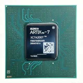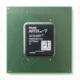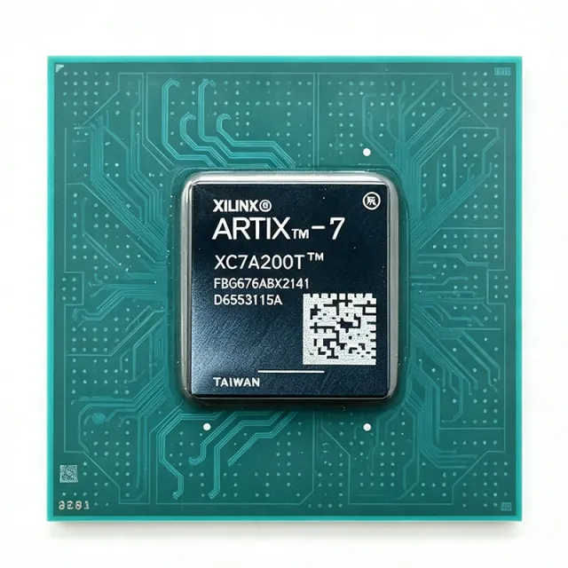
XC7A200T-2FBG676C - 740K Logic Cells FPGA | AMD Xilinx
MPN: XC7A200T-2FBG676C ✓ Active| Qty | Unit Price | Extended |
|---|---|---|
| 1 | $850 | $850.00 |
| 10 | $765 | $7,650.00 |
| 100 | $680 | $68,000.00 |
| 500 | $612 | $306,000.00 |
| 1,000 | $550 | $550,000.00 |
XC7A200T-2FBG676C Overview
An FPGA (Field-Programmable Gate Array) is a semiconductor device containing programmable logic blocks and programmable interconnects that can be configured after manufacturing to implement any digital logic function. FPGAs sit within the broader hierarchy of programmable logic devices (PLDs), which are a subset of integrated circuits (ICs). Unlike fixed-function ASICs, FPGAs offer reconfigurability, making them ideal for prototyping, rapid iteration, and applications requiring in-field updates. The Artix-7 family is optimized for cost-sensitive, high-volume applications requiring high logic density and low power.
Key features include 740K logic cells, 215K logic slices, 13 Mb of block RAM, 740 DSP slices, and 16 high-speed transceivers supporting up to 6.6 Gbps. The device also integrates a 12-bit 1 MSPS ADC (XADC) for on-chip temperature and voltage monitoring. The FBG676 package provides 400 user I/O pins with support for multiple I/O standards, enabling flexible board design.
The XC7A200T-2FBG676C is built on the 28nm high-k metal gate (HKMG) process technology, balancing performance and power efficiency. The -2 speed grade offers a balance of performance and cost, with internal clock speeds up to 628 MHz. The device supports partial reconfiguration, allowing dynamic updates to specific logic regions without disrupting the entire design.
Typical applications include software-defined radio (SDR), medical imaging, industrial motor control, and high-performance computing acceleration. The high logic density and DSP slices make it suitable for digital signal processing (DSP) tasks such as FFTs and filters, while the transceivers enable high-speed serial communication in networking equipment.
When designing with this FPGA, ensure adequate decoupling capacitors on all power rails (VCCINT, VCCAUX, VCCO) and follow the recommended power-up sequence. The configuration interface (JTAG, SPI, or BPI) must be carefully planned to support the required boot mode and update strategy.
Drop-in alternatives for XC7A200T-2FBG676C — same package, pin-to-pin compatible. Different-package parts requiring PCB rework are excluded.
Variants in this series
Same-series models that are drop-in compatible with XC7A200T-2FBG676C (same form factor and footprint) — differing in Operating Temperature, Package, Transceivers.
Quick Comparison Tool — Select alternative parts for side-by-side comparison:
XC7A200T-2FBG676I
✓ In Stock
$100 / Unit
View Datasheet →XC7A200T-1FBG676C
📋 Reference alternative (not in catalog)
XC7A200T-3FBG676C
📋 Reference alternative (not in catalog)
XC7A200T-2FBG676C Maximum Ratings & Electrical Characteristics
| Family | Artix-7 |
| Logic Cells | 740K |
| Logic Slices | 215K |
| Block RAM | 13 Mb |
| DSP Slices | 740 |
| Transceivers | 16 (up to 6.6 Gbps) |
| User I/O | 400 |
| Core Voltage | 1.0V |
| I/O Standards | LVCMOS, LVDS, HSTL, SSTL |
| Speed Grade | -2 |
| Package | FCBGA-676 (FBG676) |
| Operating Temperature | 0C to +85C |
| Configuration | JTAG, SPI, BPI |
| ADC | 12-bit 1 MSPS XADC |
| Process Technology | 28nm HKMG |
XC7A200T-2FBG676C Pin Configuration
| Pin A1 | IO_L1P_T0_100 — User I/O bank 100 |
| Pin A2 | IO_L1N_T0_100 — User I/O bank 100 |
| Pin B1 | IO_L2P_T0_100 — User I/O bank 100 |
| Pin B2 | IO_L2N_T0_100 — User I/O bank 100 |
| Pin C1 | VCCINT — Core voltage 1.0V |
| Pin C2 | GND — Ground |
| Pin D1 | VCCAUX — Auxiliary voltage 1.8V |
| Pin D2 | GND — Ground |
| Pin E1 | IO_L3P_T0_100 — User I/O bank 100 |
| Pin E2 | IO_L3N_T0_100 — User I/O bank 100 |
| Pin F1 | IO_L4P_T0_100 — User I/O bank 100 |
| Pin F2 | IO_L4N_T0_100 — User I/O bank 100 |
Typical Applications
XC7A200T-2FBG676C is suitable for 6 applications: Software-Defined Radio (SDR), Medical Imaging, Industrial Motor Control, High-Performance Computing (HPC) Acceleration, Video Processing and Surveillance, Aerospace and Defense.
Software-Defined Radio (SDR)
The XC7A200T-2FBG676C is ideal for SDR platforms due to its 740 DSP slices and 16 high-speed transceivers. In a typical SDR, the FPGA handles digital down-conversion (DDC), channel filtering, and modulation/demodulation. The DSP slices implement efficient FIR filters and FFTs, while the transceivers interface with high-speed ADCs/DACs at up to 6.6 Gbps. The 13 Mb block RAM supports large sample buffers and waveform tables. Compared to using discrete DSPs, the FPGA provides reconfigurability for multi-standard support (e.g., LTE, Wi-Fi, custom waveforms) without hardware changes. Power consumption is optimized by the 28nm process, enabling portable or battery-operated SDR units. Designers should allocate sufficient clock resources for the DDC chain and use the XADC for temperature monitoring to prevent thermal throttling.
Recommended
Medical Imaging
The XC7A200T-2FBG676C is well-suited for medical imaging systems such as ultrasound and CT scanners. Its 740K logic cells enable complex image processing pipelines, including beamforming, filtering, and image enhancement. The 740 DSP slices accelerate convolution and correlation operations, while the 13 Mb block RAM stores image frames and intermediate results. The 400 user I/O pins interface with multiple sensor arrays and memory devices. The FPGA's reconfigurability allows algorithm updates for new imaging modalities without hardware redesign. The -2 speed grade provides sufficient performance for real-time processing at 30 frames per second. Designers should implement efficient memory hierarchies to avoid bottlenecks and use the XADC for monitoring power supply integrity in safety-critical applications.
Recommended
Industrial Motor Control
The XC7A200T-2FBG676C is used in advanced motor control systems for robotics and industrial automation. Its high logic density supports complex field-oriented control (FOC) algorithms with multiple axes. The 740 DSP slices implement PID controllers, Clarke/Park transforms, and space-vector modulation (SVM). The 400 I/O pins interface with encoders, current sensors, and gate drivers. The FPGA's deterministic timing ensures precise PWM generation with minimal jitter, improving motor efficiency. The 28nm process keeps power dissipation low, allowing operation in sealed enclosures. Designers should use the XADC for real-time current and voltage monitoring to implement protection features. The transceivers can be used for high-speed communication with PLCs or robot controllers.
Recommended
High-Performance Computing (HPC) Acceleration
The XC7A200T-2FBG676C is employed as a hardware accelerator in HPC systems for tasks like genomics, financial modeling, and scientific simulations. Its 740K logic cells allow implementation of custom arithmetic units and dataflow engines. The 740 DSP slices accelerate floating-point operations when combined with external soft IP. The 13 Mb block RAM provides high-bandwidth storage for intermediate results, reducing memory latency. The 16 transceivers enable high-speed interconnect to host CPUs or other FPGAs via PCIe or Ethernet. The FPGA's reconfigurability allows the same hardware to be repurposed for different algorithms, maximizing utilization. Designers should carefully partition the design to balance logic and DSP usage, and use the XADC for thermal management in dense compute environments.
Recommended
Video Processing and Surveillance
The XC7A200T-2FBG676C is used in video surveillance systems for real-time processing of multiple camera feeds. Its 740K logic cells support video scaling, color space conversion, and object detection algorithms. The 740 DSP slices accelerate filtering and feature extraction, while the 13 Mb block RAM stores frame buffers. The 400 I/O pins interface with MIPI CSI-2 or LVDS camera sensors and HDMI/DisplayPort outputs. The FPGA's parallel processing capability enables simultaneous analysis of 4K video streams at 60 fps. The -2 speed grade provides sufficient bandwidth for high-resolution video. Designers should implement efficient DMA engines to move data between the FPGA and external DDR memory, and use the XADC for monitoring power rails in outdoor installations.
Recommended
Aerospace and Defense
The XC7A200T-2FBG676C is used in aerospace and defense systems for radar, electronic warfare, and secure communications. Its high logic density and DSP slices enable complex signal processing algorithms such as pulse compression and beamforming. The 16 transceivers support high-speed data links for radar arrays and communication systems. The FPGA's reconfigurability allows in-field updates for new threat signatures or communication protocols. The -2 speed grade provides the performance needed for real-time processing in harsh environments. Designers should implement redundancy and error correction for reliability, and use the XADC for monitoring in extreme temperature conditions. The commercial temperature grade (C) is suitable for controlled environments, while the industrial grade (I) is recommended for external deployments.
Recommended
Recommended Products Summary
Engineering reference data for XC7A200T-2FBG676C — comparison, design guidance, and compliance information.
Selection Guide
Comparison with Alternatives
| Parameter | This Product | XC7A200T-1FBG676C | XC7A200T-2FBG676I | XC7A200T-3FBG676C |
|---|---|---|---|---|
| Package | FCBGA-676 (FBG676) | FCBGA-676 (FBG676) - same | FCBGA-676 (FBG676) - same | FCBGA-676 (FBG676) - same |
| Logic Cells | 740K | 740K | 740K | 740K |
| Speed Grade | -2 | -1 | -2 | -3 |
| Operating Temperature | 0C to +85C | 0C to +85C | -40C to +100C | 0C to +85C |
| Max Clock Frequency | 628 MHz | 550 MHz | 628 MHz | 700 MHz |
| Block RAM | 13 Mb | 13 Mb | 13 Mb | 13 Mb |
| DSP Slices | 740 | 740 | 740 | 740 |
| Transceivers | 16 (6.6 Gbps) | 16 (6.6 Gbps) | 16 (6.6 Gbps) | 16 (6.6 Gbps) |
Key Differentiators
- Higher speed grade than -1 variant (vs XC7A200T-1FBG676C)
- Commercial temperature range (vs XC7A200T-2FBG676I)
- Balanced performance-cost (vs XC7A200T-3FBG676C)
Design Notes
The XC7A200T-2FBG676C requires multiple power rails: VCCINT at 1.0V, VCCAUX at 1.8V, and VCCO depending on I/O banks (1.2V to 3.3V). Use low-impedance power distribution with dedicated power planes. Place 100nF and 10uF decoupling capacitors close to each power pin. Follow the recommended power-up sequence: VCCINT, then VCCAUX, then VCCO. Use the XADC to monitor on-chip temperatures and voltages for reliable operation.
The FBG676 package has a 1.0mm ball pitch, requiring high-density PCB routing. Use at least 4 layers with dedicated ground and power planes. For high-speed transceivers, use controlled impedance traces (50 ohm single-ended, 100 ohm differential) and minimize via stubs. Place transceiver power supply filters close to the FPGA. Follow the layout guidelines in UG583 for optimal signal integrity.
Ensure the configuration mode pins (M[2:0]) are set correctly for the desired boot interface (JTAG, SPI, or BPI). Do not leave unused I/O pins floating - configure them as inputs with pull-ups or drive them to a defined state. Verify that the VCCO voltage matches the I/O standard used. For designs using partial reconfiguration, ensure the PR regions are properly isolated and the bitstreams are compatible.
Compliance Information
RoHS compliant per AMD Xilinx product page. Not AEC-Q100 qualified as it is not an automotive-grade device.