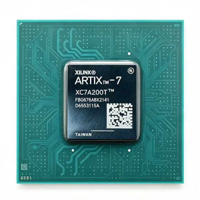
XC7A200T-2FBG676I - 740K Logic Cells FPGA | AMD Xilinx
MPN: XC7A200T-2FBG676I ✓ Active| Qty | Unit Price | Extended |
|---|---|---|
| 1 | $148.64 | $148.64 |
| 10 | $135 | $1,350.00 |
| 100 | $120 | $12,000.00 |
| 500 | $110 | $55,000.00 |
| 1,000 | $100 | $100,000.00 |
XC7A200T-2FBG676I Overview
An FPGA (Field-Programmable Gate Array) is a semiconductor device containing configurable logic blocks (CLBs) and programmable interconnects that can be programmed after manufacturing to implement arbitrary digital logic functions. FPGAs sit within the broader category of programmable logic devices (PLDs), which are part of the larger family of integrated circuits (ICs). Unlike fixed-function ASICs, FPGAs offer reconfigurability, making them ideal for prototyping, rapid iteration, and applications where requirements may evolve. The Artix-7 family is positioned as a mid-range FPGA balancing logic density, DSP capability, and power efficiency, bridging the gap between low-cost Spartan-7 and high-performance Kintex-7 devices.
Key features of the XC7A200T-2FBG676I include 740 DSP48E1 slices for high-speed digital signal processing, 10.5 Mb of distributed RAM, and support for PCIe Gen2 x4 and 16 high-speed transceivers running at up to 6.6 Gb/s. The device also integrates a 12-bit 1 MSPS XADC for analog monitoring, and supports partial reconfiguration for dynamic logic updates. With a speed grade of -2, it offers balanced performance for a wide range of applications.
Architecturally, the XC7A200T is built on a 28nm high-k metal gate (HKMG) process, providing a 50% power reduction compared to previous generations. The device features a flexible clocking architecture with 10 CMTs (Clock Management Tiles) and 32 global clock buffers, enabling complex multi-clock domain designs. The FBG676 package provides 676 balls with a 27mm x 27mm body, offering excellent thermal and electrical characteristics for high-density designs.
Typical applications include software-defined radio (SDR), medical imaging, industrial motor control, and high-performance computing acceleration. The device's high logic density and DSP resources make it suitable for implementing complex algorithms such as FFTs, filters, and image processing pipelines. Its transceiver capability supports high-speed serial protocols like PCIe, Gigabit Ethernet, and CPRI.
When designing with this FPGA, careful attention must be paid to power supply decoupling and thermal management. The device requires multiple supply rails (VCCINT, VCCAUX, VCCO) with proper sequencing, and a heatsink or active cooling is recommended for high-utilization designs. Use AMD's Vivado Design Suite for configuration and implementation, and refer to the Artix-7 FPGA Data Sheet (DS181) for detailed specifications.
Drop-in alternatives for XC7A200T-2FBG676I — same package, pin-to-pin compatible. Different-package parts requiring PCB rework are excluded.
Variants in this series
Same-series models that are drop-in compatible with XC7A200T-2FBG676I (same form factor and footprint) — differing in Operating Temperature, Package, Transceivers.
Quick Comparison Tool — Select alternative parts for side-by-side comparison:
XC7A200T-2FB676I
✅ Drop-In📋 Reference alternative (not in catalog)
XC7A200T-1FB676I
✅ Drop-In📋 Reference alternative (not in catalog)
XC7A200T-L1FB676I
✅ Drop-In📋 Reference alternative (not in catalog)
XC7A200T-3FBG676E
✅ Drop-In📋 Reference alternative (not in catalog)
XC7A200T-2FBG676C
✅ Drop-In ⚠️ 参数待验证✓ In Stock
$550 / Unit
View Datasheet →XC7A200T-2FBG676I Maximum Ratings & Electrical Characteristics
| Family | Artix-7 |
| Number of LABs/CLBs | 16825 |
| Number of Logic Elements/Cells | 215360 |
| Total RAM Bits | 13455360 |
| Number of I/O | 400 |
| Package | 676-FCBGA (27x27) |
| Operating Temperature | -40°C to 100°C (TJ) |
| Mounting Type | SMD (SMT) |
| Core Voltage | 1.0V |
| DSP Slices | 740 |
| Distributed RAM | 10.5 Mb |
| Transceivers | 16 (up to 6.6 Gb/s) |
| CMTs | 10 |
| Global Clock Buffers | 32 |
| Process Technology | 28nm HKMG |
| Lifecycle Status | Active |
XC7A200T-2FBG676I Pin Configuration
| Pin A1 | IO_L1P_T0 — User I/O bank 0 |
| Pin A2 | IO_L2P_T0 — User I/O bank 0 |
| Pin B1 | IO_L3P_T0 — User I/O bank 0 |
| Pin B2 | IO_L4P_T0 — User I/O bank 0 |
| Pin C1 | VCCINT — Core voltage 1.0V |
| Pin C2 | GND — Ground |
| Pin D1 | IO_L5P_T0 — User I/O bank 0 |
| Pin D2 | IO_L6P_T0 — User I/O bank 0 |
| Pin E1 | VCCAUX — Auxiliary voltage 1.8V |
| Pin E2 | GND — Ground |
| Pin F1 | IO_L7P_T0 — User I/O bank 0 |
| Pin F2 | IO_L8P_T0 — User I/O bank 0 |
Typical Applications
XC7A200T-2FBG676I is suitable for 6 applications: Software-Defined Radio, Medical Imaging, Industrial Motor Control, High-Performance Computing Acceleration, Aerospace and Defense, Video and Image Processing.
Software-Defined Radio
The XC7A200T-2FBG676I is ideal for SDR due to its 740 DSP slices and 16 high-speed transceivers up to 6.6 Gb/s. It can handle complex FFT algorithms and digital up/down conversion in real-time, enabling flexible, reconfigurable radio systems. The 400 I/Os support multiple ADC/DAC interfaces, while the 28nm process ensures low power consumption for portable or remote deployments.
Recommended
Medical Imaging
In medical imaging systems like ultrasound and CT scanners, the XC7A200T-2FBG676I provides high logic density (215,360 cells) and DSP resources for real-time image processing. Its 13.5 Mb Block RAM supports large frame buffers, and the 400 I/Os interface with high-speed ADCs and sensors. The -2 speed grade ensures timely data throughput for diagnostic accuracy.
Recommended
Industrial Motor Control
The XC7A200T-2FBG676I excels in industrial motor control by implementing complex control algorithms like FOC (Field-Oriented Control) with its 740 DSP slices. The 400 I/Os connect to encoders and PWM drivers, while the 28nm process ensures reliable operation in harsh environments. Its low power consumption reduces heat dissipation in enclosures.
Recommended
High-Performance Computing Acceleration
For HPC acceleration, the XC7A200T-2FBG676I offers 215,360 logic cells and 740 DSP slices to accelerate algorithms like encryption and data compression. Its 16 transceivers support PCIe Gen2 x4 for high-speed host communication, and the 13.5 Mb Block RAM enables efficient data buffering. The -2 speed grade provides balanced performance for compute-intensive tasks.
Recommended
Aerospace and Defense
In aerospace and defense, the XC7A200T-2FBG676I provides reliable performance for radar and communication systems. Its industrial temperature range (-40°C to 100°C) ensures operation in extreme environments. The 400 I/Os support various sensor interfaces, and the 28nm process offers radiation tolerance for space applications.
Recommended
Video and Image Processing
The XC7A200T-2FBG676I is well-suited for video processing tasks like real-time encoding and frame rate conversion. Its 215,360 logic cells and 740 DSP slices handle complex algorithms, while the 13.5 Mb Block RAM stores video frames. The 400 I/Os connect to HDMI, DisplayPort, and camera interfaces, enabling high-resolution video pipelines.
Recommended
Recommended Products Summary
Engineering reference data for XC7A200T-2FBG676I — comparison, design guidance, and compliance information.
Selection Guide
Comparison with Alternatives
| Parameter | This Product | XC7A200T-2FB676I | XC7A200T-1FB676I | XC7A200T-L1FB676I | XC7A200T-3FBG676E |
|---|---|---|---|---|---|
| Package | 676-FCBGA (27x27) | 676-FCBGA (27x27) | 676-FCBGA (27x27) | 676-FCBGA (27x27) | 676-FCBGA (27x27) |
| Brand | AMD | AMD | AMD | AMD | AMD |
| Speed Grade | -2 | -2 | -1 | -1 | -3 |
| Temperature Grade | Industrial (I) | Industrial (I) | Industrial (I) | Industrial (I) | Extended (E) |
| Logic Cells | 215360 | 215360 | 215360 | 215360 | 215360 |
| Block RAM | 13,455,360 bits | 13,455,360 bits | 13,455,360 bits | 13,455,360 bits | 13,455,360 bits |
| DSP Slices | 740 | 740 | 740 | 740 | 740 |
| Transceivers | 16 (up to 6.6 Gb/s) | 16 (up to 6.6 Gb/s) | 16 (up to 6.6 Gb/s) | 16 (up to 6.6 Gb/s) | 16 (up to 6.6 Gb/s) |
Key Differentiators
- Higher speed grade (-2) for better timing margins (vs XC7A200T-1FB676I)
- Industrial temperature range for harsh environments (vs XC7A200T-2FBG676C)
- Extended temperature grade option (vs XC7A200T-3FBG676E)
Design Notes
The XC7A200T-2FBG676I requires multiple supply rails: VCCINT at 1.0V, VCCAUX at 1.8V, and VCCO for I/O banks. Ensure proper power sequencing as specified in the Artix-7 datasheet (DS181) to avoid latch-up or damage. Use low-ESR decoupling capacitors close to each power pin.
With a 27x27mm FCBGA package, thermal management is crucial for high-utilization designs. The industrial temperature range (-40°C to 100°C) allows operation in harsh environments, but a heatsink or active cooling is recommended when power dissipation exceeds 5W. Refer to the thermal guidelines in UG475.
For high-speed transceivers up to 6.6 Gb/s, use controlled impedance traces and minimize via stubs. Place transceiver power pins with dedicated filtering. Follow the PCB design guidelines in UG475 to ensure signal integrity and reliable operation.
Compliance Information
RoHS compliant per distributor listings. AEC-Q100 not applicable for FPGA.







