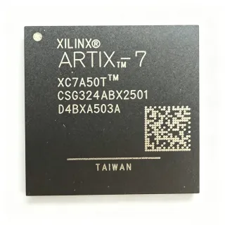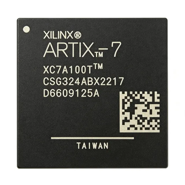
XC7A100T-2CSG324I - Artix-7 FPGA, 101K Logic Cells | AMD Xilinx
MPN: XC7A100T-2CSG324I ✓ Active| Qty | Unit Price | Extended |
|---|---|---|
| 1 | $154.61 | $154.61 |
| 10 | $142.5 | $1,425.00 |
| 100 | $128 | $12,800.00 |
| 500 | $115 | $57,500.00 |
| 1,000 | $105 | $105,000.00 |
XC7A100T-2CSG324I Overview
An FPGA (Field-Programmable Gate Array) is a semiconductor device containing a matrix of configurable logic blocks (CLBs) connected by programmable interconnects, allowing designers to implement custom digital logic circuits after manufacturing. FPGAs sit within the broader category of programmable logic devices (PLDs), which are part of the larger family of integrated circuits (ICs). Unlike fixed-function ASICs, FPGAs offer reconfigurability, enabling rapid prototyping and field upgrades, making them essential in applications ranging from embedded vision to software-defined radio.
Key features of the XC7A100T-2CSG324I include 285,120 flip-flops, 240 DSP48E1 slices (each capable of 25x18 multiplication), and 135 Block RAM blocks (36 Kb each) totaling 4,860 Kb. The device supports up to 300 user I/O pins with support for multiple I/O standards including LVCMOS, LVDS, and HSTL. It integrates a 12-bit, 1 MSPS XADC for analog monitoring and supports PCIe Gen2 x1 and 10/100/1000 Ethernet via hardened blocks. The -2 speed grade provides balanced performance, with internal clock speeds up to 628 MHz.
The Artix-7 architecture is built on a 28 nm high-k metal gate (HKMG) process, offering a 50% lower static power compared to previous generations. The device includes a unified configuration interface supporting JTAG, SelectMAP, and Quad-SPI flash programming. Its low-power transceivers (up to 16 GTP transceivers at 6.6 Gbps) enable high-speed serial connectivity for applications like video over SDI and CPRI.
Typical applications include software-defined radio (SDR), medical imaging, motor control, and industrial Ethernet. The XC7A100T-2CSG324I is particularly suited for designs requiring high logic density with moderate I/O counts, such as camera-based vision systems and test equipment. Its industrial temperature grade makes it reliable for harsh environments.
For detailed specifications, refer to the official AMD Xilinx datasheet (DS181) and the Artix-7 FPGA product page at https://www.xilinx.com/products/silicon-devices/fpga/artix-7.html. When designing with this FPGA, careful attention must be paid to power supply decoupling and PCB layout to ensure signal integrity at high speeds. The device requires multiple supply rails (VCCINT, VCCAUX, VCCO) with specific sequencing, and the use of the XADC for thermal monitoring is recommended to prevent overheating.
Drop-in alternatives for XC7A100T-2CSG324I — same package, pin-to-pin compatible. Different-package parts requiring PCB rework are excluded.
Variants in this series
Same-series models that are drop-in compatible with XC7A100T-2CSG324I (same form factor and footprint) — differing in Package, Operating Temperature, Block RAM, Logic Cells, Core Voltage.
Quick Comparison Tool — Select alternative parts for side-by-side comparison:
XC7A100T-2CSG324C
✅ Drop-In✓ In Stock
$59.5 / Unit
View Datasheet →XC7A100T-1CSG324C
✅ Drop-In✓ In Stock
$59.9 / Unit
View Datasheet →XC7A100T-1CSG324I
✅ Drop-In ⚠️ 参数待验证✓ In Stock
$59.9 / Unit
View Datasheet →XC7A100T-3CSG324I
✅ Drop-In ⚠️ 参数待验证📋 Reference alternative (not in catalog)
XC7A100T-2CSG324C
✅ Drop-In✓ In Stock
$59.5 / Unit
View Datasheet →XC7A100T-2CSG324I Maximum Ratings & Electrical Characteristics
| Family | Artix-7 |
| Number of Logic Elements/Cells | 101440 |
| Number of LABs/CLBs | 7925 |
| Total RAM Bits | 4976640 |
| Number of I/O | 210 |
| Number of DSP Slices | 240 |
| Number of Block RAM Blocks | 135 (36 Kb each) |
| Number of Flip-Flops | 285120 |
| Number of GTP Transceivers | 16 (up to 6.6 Gbps) |
| Operating Supply Voltage | 0.95 V ~ 1.05 V |
| Operating Temperature Range | -40°C ~ +100°C (TJ) |
| Package | 324-LFBGA, CSPBGA (CSG324) |
| Mounting Type | Surface Mount |
| Speed Grade | -2 |
| Internal Clock Speed | Up to 628 MHz |
| Process Technology | 28 nm HKMG |
| Configuration Interface | JTAG, SelectMAP, Quad-SPI |
| XADC | 12-bit, 1 MSPS |
| PCIe Support | Gen2 x1 |
| Ethernet Support | 10/100/1000 Mbps |
XC7A100T-2CSG324I Pin Configuration
| Pin A1 | IO_L1P_T0 — User I/O bank 0, differential pair P |
| Pin A2 | IO_L1N_T0 — User I/O bank 0, differential pair N |
| Pin B1 | IO_L2P_T0 — User I/O bank 0, differential pair P |
| Pin B2 | IO_L2N_T0 — User I/O bank 0, differential pair N |
| Pin C1 | VCCINT — Core logic supply voltage (0.95V-1.05V) |
| Pin C2 | GND — Ground |
| Pin D1 | VCCAUX — Auxiliary supply voltage (1.8V) |
| Pin D2 | VCCO_0 — I/O bank 0 supply voltage |
| Pin E1 | IO_L3P_T0 — User I/O bank 0, differential pair P |
| Pin E2 | IO_L3N_T0 — User I/O bank 0, differential pair N |
| Pin F1 | IO_L4P_T0 — User I/O bank 0, differential pair P |
| Pin F2 | IO_L4N_T0 — User I/O bank 0, differential pair N |
| Pin G1 | DONE — Configuration done indicator |
| Pin G2 | PROG_B — Configuration program pin (active low) |
| Pin H1 | M[2:0] — Configuration mode select pins |
| Pin H2 | TCK — JTAG clock |
| Pin J1 | TDI — JTAG data input |
| Pin J2 | TDO — JTAG data output |
| Pin K1 | TMS — JTAG mode select |
| Pin K2 | VCCBATT — Battery backup voltage for key memory |
Typical Applications
XC7A100T-2CSG324I is suitable for 6 applications: Software-Defined Radio (SDR), Medical Imaging, Motor Control, Industrial Ethernet, Video over SDI, Test and Measurement.
Software-Defined Radio (SDR)
The XC7A100T-2CSG324I is ideal for SDR applications due to its 240 DSP48E1 slices and 16 GTP transceivers at 6.6 Gbps. The DSP slices handle complex modulation/demodulation algorithms, while the transceivers enable high-speed data conversion interfaces. The industrial temperature range ensures reliable operation in field-deployed radios. The 4,860 Kb of block RAM supports large FFT buffers and filter coefficients, enabling real-time signal processing.
Recommended
Medical Imaging
The XC7A100T-2CSG324I excels in medical imaging systems like ultrasound and CT scanners, where high logic density and DSP capabilities are essential. Its 101,440 logic cells implement image processing pipelines, while 240 DSP slices accelerate filtering and beamforming algorithms. The 12-bit XADC monitors system health, and the industrial temperature range ensures reliability in clinical environments. The 210 I/O pins interface with image sensors and display controllers.
Recommended
Motor Control
The XC7A100T-2CSG324I is well-suited for motor control applications, offering 240 DSP slices for implementing complex control algorithms like FOC (Field-Oriented Control). The 210 I/O pins interface with encoders, current sensors, and gate drivers. The industrial temperature range (-40°C to +100°C) ensures operation in factory environments. The 4,860 Kb of block RAM stores control tables and diagnostic data, while the XADC monitors motor currents and temperatures.
Recommended
Industrial Ethernet
The XC7A100T-2CSG324I supports 10/100/1000 Ethernet via hardened blocks, making it ideal for industrial Ethernet applications like PROFINET and EtherCAT. The 16 GTP transceivers enable high-speed backplane communication, while the 101,440 logic cells implement protocol stacks and real-time control logic. The industrial temperature range ensures reliable operation in factory floors. The 210 I/O pins interface with PHY chips and industrial fieldbus transceivers.
Recommended
Video over SDI
The XC7A100T-2CSG324I is ideal for video over SDI (Serial Digital Interface) applications, with 16 GTP transceivers supporting 6.6 Gbps for 3G-SDI and 12G-SDI. The 101,440 logic cells implement video processing pipelines, color space conversion, and frame buffering. The 4,860 Kb of block RAM stores video frames for processing. The industrial temperature range ensures reliable operation in broadcast environments.
Recommended
Test and Measurement
The XC7A100T-2CSG324I is well-suited for test and measurement equipment like oscilloscopes and logic analyzers. Its 101,440 logic cells implement acquisition and triggering logic, while 240 DSP slices handle signal processing. The 12-bit XADC provides analog monitoring, and the 210 I/O pins interface with high-speed ADCs and DACs. The industrial temperature range ensures accuracy in lab and field environments.
Recommended
Recommended Products Summary
Engineering reference data for XC7A100T-2CSG324I — comparison, design guidance, and compliance information.
Selection Guide
Comparison with Alternatives
| Parameter | This Product | XC7A100T-2CSG324C | XC7A100T-1CSG324C | XC7A100T-1CSG324I | XC7A100T-3CSG324I | XC7A200T-2FFG1156C |
|---|---|---|---|---|---|---|
| Package | 324-LFBGA, CSPBGA (CSG324) | 324-LFBGA, CSPBGA (CSG324) - same | 324-LFBGA, CSPBGA (CSG324) - same | 324-LFBGA, CSPBGA (CSG324) - same | 324-LFBGA, CSPBGA (CSG324) - same | 1156-FCBGA (FFG1156) - different |
| Brand | AMD | AMD | AMD | AMD | AMD | AMD |
| Logic Cells | 101440 | 101440 | 101440 | 101440 | 101440 | 215360 |
| DSP Slices | 240 | 240 | 240 | 240 | 240 | 740 |
| Block RAM (Kb) | 4860 | 4860 | 4860 | 4860 | 4860 | 13140 |
| Number of I/O | 210 | 210 | 210 | 210 | 210 | 500 |
| Speed Grade | -2 | -2 | -1 | -1 | -3 | -2 |
| Temperature Range | -40°C to +100°C (Industrial) | 0°C to +85°C (Commercial) | 0°C to +85°C (Commercial) | -40°C to +100°C (Industrial) | -40°C to +100°C (Industrial) | 0°C to +85°C (Commercial) |
| GTP Transceivers | 16 (up to 6.6 Gbps) | 16 (up to 6.6 Gbps) | 16 (up to 6.6 Gbps) | 16 (up to 6.6 Gbps) | 16 (up to 6.6 Gbps) | 16 (up to 6.6 Gbps) |
Key Differentiators
- Industrial temperature range (vs XC7A100T-2CSG324C)
- Balanced speed grade (-2) (vs XC7A100T-1CSG324C)
- Cost-effective logic density (vs XC7A200T-2FFG1156C)
Design Notes
The XC7A100T-2CSG324I requires multiple supply rails: VCCINT (0.95V-1.05V), VCCAUX (1.8V), and VCCO (per I/O bank). Use low-dropout regulators or switching regulators with proper decoupling. Place 100nF and 10uF capacitors close to each power pin. Follow the power sequencing requirements in the datasheet to avoid damage.
For high-speed signals up to 6.6 Gbps, use controlled impedance traces (50 ohm single-ended, 100 ohm differential). Keep trace lengths matched for differential pairs. Use ground planes under all high-speed routing. Refer to UG475 for package pinout and PCB design guidelines.
The industrial temperature range (-40°C to +100°C) requires careful thermal management. Use thermal vias under the exposed pad to conduct heat to the PCB ground plane. For high utilization designs, consider adding a heatsink or forced airflow. Monitor junction temperature using the XADC.
Compliance Information
RoHS compliant per AMD Xilinx product page. Not AEC-Q100 qualified - this is an FPGA, not an automotive-grade component. Halogen-free status not specified in available data.