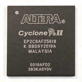
EPM570F256C5NRR - MAX II CPLD, 570 LEs, 256-BGA | Intel
MPN: EPM570F256C5NRR ✓ Active| Qty | Unit Price | Extended |
|---|---|---|
| 1 | $18.5 | $18.50 |
| 10 | $17.1 | $171.00 |
| 100 | $15.45 | $1,545.00 |
| 500 | $13.8 | $6,900.00 |
| 1,000 | $12.2 | $12,200.00 |
| 3,000 | $10.9 | $32,700.00 |
Drop-in alternatives for EPM570F256C5NRR — same package, pin-to-pin compatible. Different-package parts requiring PCB rework are excluded.
Quick Comparison Tool — Select alternative parts for side-by-side comparison:
EPM570F256C5N
✅ Drop-In✓ In Stock
$17.03 / Unit
View Datasheet →EPM570F256C5
✅ Drop-In✓ In Stock
$7.1 / Unit
View Datasheet →EPM570F256C4N
✅ Drop-In✓ In Stock
$26.85 / Unit
View Datasheet →EPM570F256C3N
✅ Drop-In✓ In Stock
$13.75 / Unit
View Datasheet →EPM570F256C5NRR Maximum Ratings & Electrical Characteristics
| Series | MAX II |
| Family | MAX II (CPLD) |
| Logic Elements | 570 |
| Macro Cells | 440 |
| Pin-to-Pin Delay (tPD) | 8.7 ns (C5 speed grade) |
| Internal fMAX | 201.1 MHz |
| User Flash Memory (UFM) | 8 Kbytes |
| Maximum User I/O Pins | 212 (typical, 256-BGA) |
| Operating Supply Voltage - Core (VCCINT) | 2.5 V (3.3 V tolerant) |
| Operating Supply Voltage - I/O (VCCIO) | 2.5 V or 3.3 V |
| Process Technology | 0.18 µm flash CMOS |
| Package | 256-ball FBGA (FineLine BGA) |
| Mounting Type | Surface Mount |
| Operating Temperature | 0 °C to +85 °C (commercial, C-speed grade) |
| Programming Interface | JTAG (IEEE 1149.1), in-system programmable |
| Configuration Memory | On-chip non-volatile flash |
| RoHS Status | Compliant |
EPM570F256C5NRR Pin Configuration
| Pin A1 | I/O — General-purpose user I/O (bank 1) |
| Pin A2 | I/O — General-purpose user I/O (bank 1) |
| Pin A3 | VCCIO1 — I/O bank 1 supply (2.5V or 3.3V) |
| Pin A4 | I/O — General-purpose user I/O |
| Pin A5 | GND — Ground |
| Pin A6 | I/O — General-purpose user I/O (bank 2) |
| Pin A7 | I/O — General-purpose user I/O (bank 2) |
| Pin A8 | VCCIO2 — I/O bank 2 supply (2.5V or 3.3V) |
| Pin B1 | I/O — General-purpose user I/O |
| Pin B2 | I/O — General-purpose user I/O |
| Pin B3 | GND — Ground |
| Pin B4 | I/O — General-purpose user I/O |
| Pin B5 | VCCINT — Core supply (2.5V) |
| Pin B6 | I/O — General-purpose user I/O |
| Pin B7 | GND — Ground |
| Pin B8 | I/O — General-purpose user I/O |
| Pin C1 | I/O — General-purpose user I/O (bank 1) |
| Pin C2 | I/O — General-purpose user I/O (bank 1) |
| Pin C3 | I/O — General-purpose user I/O (bank 1) |
| Pin C4 | nCONFIG — Configuration control (active low) |
| Pin C5 | I/O — General-purpose user I/O |
| Pin C6 | I/O — General-purpose user I/O (bank 2) |
| Pin C7 | I/O — General-purpose user I/O (bank 2) |
| Pin C8 | I/O — General-purpose user I/O (bank 2) |
Safe Operating Area (SOA) & Thermal Characteristics
No official SOA curve available for this digital IC. Always operate within absolute maximum ratings specified in the datasheet. Ensure adequate cooling and derate as needed.
Typical Applications
EPM570F256C5NRR is suitable for 6 applications: Microcontroller Bus-Bridging Glue Logic, Power-Sequencer and Watchdog Controller, LED Panel Scan and PWM Controller, PCI / ISA Bus Peripheral Bridge, Industrial I/O Expansion Module, Custom Protocol Bridge (UART/SPI/I2C Multiplexer).
Microcontroller Bus-Bridging Glue Logic
The EPM570F256C5NRR's 8.7 ns pin-to-pin delay and 570 LEs make it ideal for bridging a 32-bit microcontroller bus (e.g. ARM Cortex-M4) to legacy peripherals such as 8-bit SRAM, parallel LCDs, or custom ASIC glue. With 212 user I/O and 3.3 V-tolerant inputs the device interfaces directly to 3.3 V MCUs while running an internal 2.5 V core, eliminating level shifters. Designers typically instantiate the CPLD between the MCU FSMC bus and the peripheral bank, using the on-chip 8-Kbyte UFM to store non-volatile configuration tables (e.g. display timing parameters) that the MCU reads at boot. Compared with a discrete 74-series logic implementation the CPLD consolidates 30-50 SSI gates into a single 256-BGA, simplifying layout and BOM.
Recommended
Power-Sequencer and Watchdog Controller
The EPM570F256C5NRR's deterministic timing and instant-on non-volatile configuration make it well suited to power-sequencer ICs that must assert PG (power-good) signals in a precise order during board bring-up. Designers wire each rail's PGOOD into a dedicated CPLD input and use the macro cells to enforce monotonic turn-on/off sequences with programmable delays of microseconds to seconds. The on-chip 8-Kbyte UFM stores fault logs that survive power loss. The 8.7 ns tPD provides margin for high-speed FET gate drivers; the 2.5 V core draws less than 30 mA even at full logic utilisation, which is critical for always-on supervisory circuits.
Recommended
LED Panel Scan and PWM Controller
For large LED matrix panels, the EPM570F256C5NRR's 212 user I/O pins drive up to 16 multiplexed rows and 16 scanned columns of high-brightness LEDs, with the LABs running a 1 kHz refresh rate to eliminate visible flicker. Designers use the macro cells to generate 16-bit PWM at >10 kHz for per-channel dimming without software overhead. The 8.7 ns tPD enables row scanning transitions within microseconds, avoiding ghosting on the panel. The 0.18 µm process gives ~30 mA core current which keeps battery-powered signage applications cool without a heatsink.
Recommended
PCI / ISA Bus Peripheral Bridge
The EPM570F256C5NRR is widely used as a 33 MHz PCI/ISA bus bridge in legacy industrial PC designs where FPGAs are over-budget. With 8.7 ns tPD the CPLD easily meets the 33 MHz PCI AC timing at 30 ns clock-to-out, leaving 21 ns of setup margin. Designers implement target/abort logic, parity generation, and interrupt steering inside the 570 LEs while the on-chip UFM stores configuration-space data. The 256-BGA footprint fits standard PCI add-in card real estate.
Recommended
Industrial I/O Expansion Module
The EPM570F256C5NRR expands I/O for PLCs and industrial controllers that need more digital or analog channels than the host MCU provides. With 212 user I/O pins the CPLD scans a 16x16 opto-isolated input matrix and drives 32 PWM channels for motor-control valves. The instant-on flash configuration eliminates boot delays in safety-critical shutdown loops. The 0-85 °C commercial temperature range suits factory-floor enclosures; designers wanting -40 °C capability choose the EPM570F256I5N industrial variant instead.
Recommended
Custom Protocol Bridge (UART/SPI/I2C Multiplexer)
The EPM570F256C5NRR's 570 LEs are sufficient to implement a 4-port UART multiplexer, an SPI-to-I2C bridge, or a custom proprietary protocol converter between sensors and a host SoC. The deterministic 8.7 ns tPD ensures SPI clock generation at up to 50 MHz without jitter. Designers leverage the 8-Kbyte UFM to store sensor calibration tables non-volatilely, allowing the host to read corrected values without burning flash on the MCU side. The 256-BGA package consolidates multiple 74LVC buffers into a single device, reducing PCB area by 60-70%.
Recommended
Recommended Products Summary
Engineering reference data for EPM570F256C5NRR — comparison, design guidance, and compliance information.
Selection Guide
Comparison with Alternatives
| Parameter | This Product | EPM570F256C5N | EPM570F256C5 | EPM570F256C4N | EPM570F256C3N |
|---|---|---|---|---|---|
| Package | 256-ball FBGA | 256-ball FBGA (same) | 256-ball FBGA (same) | 256-ball FBGA (same) | 256-ball FBGA (same) |
| Brand | Intel | Intel (same) | Intel (same) | Intel (same) | Intel (same) |
| Logic Elements | 570 | 570 (same) | 570 (same) | 570 (same) | 570 (same) |
| Macro Cells | 440 | 440 (same) | 440 (same) | 440 (same) | 440 (same) |
| Speed Grade / tPD | C5 / 8.7 ns | C5 / 8.7 ns | C5 / 8.7 ns | C4 / ~7.0 ns (faster) | C3 / ~5.5 ns (fastest) |
| Operating Temperature | 0 °C to +85 °C (commercial) | 0 °C to +85 °C | 0 °C to +85 °C | 0 °C to +85 °C | 0 °C to +85 °C |
| Internal fMAX | 201.1 MHz | 201.1 MHz | 201.1 MHz | ~250 MHz | ~300 MHz |
| Packaging Format | Tape & Reel (RR suffix) | Tray | Tray (no suffix) | Tray (N suffix) | Tray (N suffix) |
| RoHS Compliance | Yes | Yes | Yes | Yes | Yes |
| Approximate Unit Price (qty 1) | USD 18.50 | USD 18.50 (same silicon) | USD 18.00 | USD 22.00 (faster grade) | USD 26.00 (fastest grade) |
Key Differentiators
- Instant-on non-volatile configuration without external boot PROM (vs EPM570F256C5N)
- Wider commercial availability in tape-and-reel orientation (vs EPM570F256C5N (tray))
- Predictable 8.7 ns tPD regardless of internal routing (vs EPM570F256C4N (faster grade))
- On-chip 8-Kbyte UFM for non-volatile user data (vs EPM240 (smaller MAX II))
Design Notes
The 256-ball FBGA package uses a 1.0 mm ball pitch with 17 x 17 ball grid (some balls depopulated). Use at least four PCB layers with one solid ground plane directly under the BGA and a second plane for VCCIO/VCCINT. Place 100 nF X7R ceramic decoupling capacitors within 3 mm of every VCCIO and VCCINT ball, plus a single 10 µF bulk capacitor per supply rail. Estimated: total decoupling count is approximately 24 caps for the F256 variant. Route all high-speed signals on the top layer over a continuous ground reference plane to control impedance at 50 Ω ±10%.
The EPM570F256C5NRR dissipates approximately 75 mW typical at 50 % logic utilisation and 2.5 V core. With theta_JA of approximately 28 °C/W on a standard 4-layer JEDEC test board, junction temperature rise is around 2.1 °C above ambient - well within the 0-85 °C commercial limit. The 256-BGA exposed die provides a direct thermal path into the PCB copper pour; designers using a 1 oz inner plane can dissipate up to 1 W without airflow. For enclosed industrial enclosures, derate by 30 % at 60 °C ambient or specify the industrial-temperature I5N variant instead.
Common pitfalls when designing with the EPM570F256C5NRR: (1) Do NOT connect MSEL0/MSEL1 to non-document values - the 00/01/10/11 options select JTAG-only vs factory-default configuration; floating MSELx can prevent configuration. (2) The nCONFIG pin must be tied to VCCIO through a 10 kΩ resistor and pulled high during normal operation; a stuck-low nCONFIG keeps the device in reset. (3) VCCINT must be 2.5 V ±5 % - driving the core from a 3.3 V rail damages the device. (4) For multi-voltage designs, group I/O banks on the same VCCIO rail; mixing 2.5 V and 3.3 V within one bank is undefined.
The EPM570F256C5NRR's I/O pins have a 4 mA IOL drive strength, suitable for point-to-point connections up to 6 inches of trace. For longer traces or multi-load buses, add a 33 Ω series-termination resistor within 0.5 inch of the CPLD pin. Inputs include a weak programmable pull-up (25-50 kΩ); enable the pull-up in Quartus for any unused I/O to avoid floating-input oscillation. The 8.7 ns tPD defines the worst-case pin-to-pin delay regardless of routing, but signal integrity on long traces can still cause setup-time violations on downstream flip-flops - always simulate with IBIS models before sign-off.
Compliance Information
RoHS and REACH compliant per Intel material declaration. AEC-Q100 not applicable - CPLD is not an automotive-qualified part; use MAX V or Cyclone IV for AEC-Q100 designs. Lead-free and halogen-free per MAX II datasheet MII5V1-1.5.