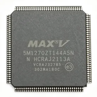
EPM7256ATI144-10N - 256-Macrocell MAX 7000A CPLD, 144-TQFP | Altera
MPN: EPM7256ATI144-10N ⚠ Last Time Buy| Qty | Unit Price | Extended |
|---|---|---|
| 1 | $49.32 | $49.32 |
| 10 | $44.5 | $445.00 |
| 100 | $39.2 | $3,920.00 |
| 500 | $34.85 | $17,425.00 |
| 1,000 | $30.1 | $30,100.00 |
Drop-in alternatives for EPM7256ATI144-10N — same package, pin-to-pin compatible. Different-package parts requiring PCB rework are excluded.
Quick Comparison Tool — Select alternative parts for side-by-side comparison:
EPM7256AETI144-10N
✅ Drop-In📋 Reference alternative (not in catalog)
EPM7256AETI144-7N
✅ Drop-In✓ In Stock
$29.81 / Unit
View Datasheet →EPM7256AETC144-10N
✅ Drop-In ⚠️ 参数待验证✓ In Stock
$15.95 / Unit
View Datasheet →EPM7256AETC144-7N
✅ Drop-In✓ In Stock
$29.75 / Unit
View Datasheet →EPM7256AETC144-5N
✅ Drop-In ⚠️ 参数待验证✓ In Stock
$9.95 / Unit
View Datasheet →EPM7256AETC144-10
✅ Drop-In ⚠️ 参数待验证✓ In Stock
$31.4 / Unit
View Datasheet →EPM7256ATI144-10N Maximum Ratings & Electrical Characteristics
| Family | MAX 7000A |
| Device Type | CPLD (Complex Programmable Logic Device) |
| Macrocells | 256 |
| Logic Array Blocks (LABs) | 16 |
| Usable Gates | 5,000 |
| Pin-to-Pin Delay | 10 ns |
| Maximum Internal Frequency | 93.5 MHz |
| Supply Voltage VCCINT | 3.3 V |
| MultiVolt I/O Voltage VCCIO | 2.5 V or 3.3 V |
| Programming Method | IEEE Std. 1149.1 JTAG (ISP) |
| Non-volatile Configuration | Yes (EEPROM) |
| Package | TQFP-144 |
| Operating Temperature | -40C to +85C (industrial) |
EPM7256ATI144-10N Pin Configuration
| Pin 1 | I/O — User I/O (bank 1) |
| Pin 2 | I/O — User I/O (bank 1) |
| Pin 3 | I/O — User I/O (bank 1) |
| Pin 4 | I/O — User I/O (bank 1) |
| Pin 5 | I/O — User I/O (bank 1) |
| Pin 6 | I/O — User I/O (bank 1) |
| Pin 7 | I/O — User I/O (bank 1) |
| Pin 8 | I/O — User I/O (bank 1) |
| Pin 9 | GND — Ground |
| Pin 10 | I/O — User I/O (bank 1) |
| Pin 11 | I/O — User I/O (bank 1) |
| Pin 12 | I/O — User I/O (bank 1) |
| Pin 13 | I/O — User I/O (bank 1) |
| Pin 14 | TDI — JTAG Test Data In |
| Pin 15 | TMS — JTAG Test Mode Select |
| Pin 16 | TCK — JTAG Test Clock |
| Pin 17 | I/O — User I/O (bank 1) |
| Pin 18 | I/O — User I/O (bank 1) |
| Pin 19 | I/O — User I/O (bank 1) |
| Pin 20 | I/O — User I/O (bank 1) |
| Pin 21 | I/O — User I/O (bank 1) |
| Pin 22 | I/O — User I/O (bank 1) |
| Pin 23 | I/O — User I/O (bank 1) |
| Pin 24 | I/O — User I/O (bank 1) |
| Pin 25 | I/O — User I/O (bank 1) |
| Pin 26 | I/O — User I/O (bank 1) |
| Pin 27 | I/O — User I/O (bank 1) |
| Pin 28 | I/O — User I/O (bank 1) |
| Pin 29 | I/O — User I/O (bank 1) |
| Pin 30 | VCCINT — Core supply 3.3V |
| Pin 31 | I/O — User I/O (bank 1) |
| Pin 32 | I/O — User I/O (bank 1) |
| Pin 33 | I/O — User I/O (bank 1) |
| Pin 34 | I/O — User I/O (bank 1) |
| Pin 35 | GND — Ground |
| Pin 36 | I/O — User I/O (bank 1) |
| Pin 37 | I/O — User I/O (bank 2) |
| Pin 38 | I/O — User I/O (bank 2) |
| Pin 39 | I/O — User I/O (bank 2) |
| Pin 40 | I/O — User I/O (bank 2) |
| Pin 41 | I/O — User I/O (bank 2) |
| Pin 42 | I/O — User I/O (bank 2) |
| Pin 43 | I/O — User I/O (bank 2) |
| Pin 44 | I/O — User I/O (bank 2) |
| Pin 45 | VCCIO1 — I/O bank 1 supply (2.5V or 3.3V) |
| Pin 46 | I/O — User I/O (bank 2) |
| Pin 47 | I/O — User I/O (bank 2) |
| Pin 48 | I/O — User I/O (bank 2) |
| Pin 49 | I/O — User I/O (bank 2) |
| Pin 50 | I/O — User I/O (bank 2) |
| Pin 51 | I/O — User I/O (bank 2) |
| Pin 52 | I/O — User I/O (bank 2) |
| Pin 53 | I/O — User I/O (bank 2) |
| Pin 54 | I/O — User I/O (bank 2) |
| Pin 55 | I/O — User I/O (bank 2) |
| Pin 56 | I/O — User I/O (bank 2) |
| Pin 57 | I/O — User I/O (bank 2) |
| Pin 58 | I/O — User I/O (bank 2) |
| Pin 59 | I/O — User I/O (bank 2) |
| Pin 60 | GND — Ground |
| Pin 61 | I/O — User I/O (bank 2) |
| Pin 62 | I/O — User I/O (bank 2) |
| Pin 63 | I/O — User I/O (bank 2) |
| Pin 64 | I/O — User I/O (bank 2) |
| Pin 65 | I/O — User I/O (bank 2) |
| Pin 66 | I/O — User I/O (bank 2) |
| Pin 67 | I/O — User I/O (bank 2) |
| Pin 68 | I/O — User I/O (bank 2) |
| Pin 69 | I/O — User I/O (bank 2) |
| Pin 70 | I/O — User I/O (bank 2) |
| Pin 71 | I/O — User I/O (bank 2) |
| Pin 72 | I/O — User I/O (bank 2) |
| Pin 73 | I/O — User I/O (bank 2) |
| Pin 74 | I/O — User I/O (bank 2) |
| Pin 75 | I/O — User I/O (bank 2) |
| Pin 76 | VCCIO2 — I/O bank 2 supply (2.5V or 3.3V) |
| Pin 77 | I/O — User I/O (bank 2) |
| Pin 78 | I/O — User I/O (bank 2) |
| Pin 79 | I/O — User I/O (bank 2) |
| Pin 80 | I/O — User I/O (bank 2) |
| Pin 81 | I/O — User I/O (bank 2) |
| Pin 82 | I/O — User I/O (bank 2) |
| Pin 83 | I/O — User I/O (bank 2) |
| Pin 84 | I/O — User I/O (bank 2) |
| Pin 85 | I/O — User I/O (bank 2) |
| Pin 86 | I/O — User I/O (bank 2) |
| Pin 87 | I/O — User I/O (bank 2) |
| Pin 88 | I/O — User I/O (bank 2) |
| Pin 89 | I/O — User I/O (bank 2) |
| Pin 90 | GND — Ground |
| Pin 91 | I/O — User I/O (bank 2) |
| Pin 92 | I/O — User I/O (bank 2) |
| Pin 93 | I/O — User I/O (bank 2) |
| Pin 94 | I/O — User I/O (bank 2) |
| Pin 95 | I/O — User I/O (bank 2) |
| Pin 96 | I/O — User I/O (bank 2) |
| Pin 97 | I/O — User I/O (bank 2) |
| Pin 98 | I/O — User I/O (bank 2) |
| Pin 99 | I/O — User I/O (bank 2) |
| Pin 100 | I/O — User I/O (bank 2) |
| Pin 101 | I/O — User I/O (bank 2) |
| Pin 102 | I/O — User I/O (bank 2) |
| Pin 103 | I/O — User I/O (bank 2) |
| Pin 104 | I/O — User I/O (bank 2) |
| Pin 105 | I/O — User I/O (bank 2) |
| Pin 106 | GND — Ground |
| Pin 107 | I/O — User I/O (bank 2) |
| Pin 108 | I/O — User I/O (bank 2) |
| Pin 109 | I/O — User I/O (bank 2) |
| Pin 110 | I/O — User I/O (bank 2) |
| Pin 111 | I/O — User I/O (bank 2) |
| Pin 112 | I/O — User I/O (bank 2) |
| Pin 113 | I/O — User I/O (bank 2) |
| Pin 114 | I/O — User I/O (bank 2) |
| Pin 115 | I/O — User I/O (bank 2) |
| Pin 116 | I/O — User I/O (bank 2) |
| Pin 117 | I/O — User I/O (bank 2) |
| Pin 118 | I/O — User I/O (bank 2) |
| Pin 119 | I/O — User I/O (bank 2) |
| Pin 120 | I/O — User I/O (bank 2) |
| Pin 121 | I/O — User I/O (bank 2) |
| Pin 122 | GND — Ground |
| Pin 123 | I/O — User I/O (bank 2) |
| Pin 124 | I/O — User I/O (bank 2) |
| Pin 125 | I/O — User I/O (bank 2) |
| Pin 126 | I/O — User I/O (bank 2) |
| Pin 127 | I/O — User I/O (bank 2) |
| Pin 128 | I/O — User I/O (bank 2) |
| Pin 129 | I/O — User I/O (bank 2) |
| Pin 130 | I/O — User I/O (bank 2) |
| Pin 131 | I/O — User I/O (bank 2) |
| Pin 132 | I/O — User I/O (bank 2) |
| Pin 133 | I/O — User I/O (bank 2) |
| Pin 134 | I/O — User I/O (bank 2) |
| Pin 135 | I/O — User I/O (bank 2) |
| Pin 136 | I/O — User I/O (bank 2) |
| Pin 137 | I/O — User I/O (bank 2) |
| Pin 138 | GND — Ground |
| Pin 139 | I/O — User I/O (bank 2) |
| Pin 140 | I/O — User I/O (bank 2) |
| Pin 141 | I/O — User I/O (bank 2) |
| Pin 142 | I/O — User I/O (bank 2) |
| Pin 143 | I/O — User I/O (bank 2) |
| Pin 144 | I/O — User I/O (bank 2) |
Safe Operating Area (SOA) & Thermal Characteristics
No official SOA curve available for this digital IC. Always operate within absolute maximum ratings specified in the datasheet. Ensure adequate cooling and derate as needed.
Typical Applications
EPM7256ATI144-10N is suitable for 6 applications: PCI / ISA Bus Address Decoding, Industrial Control Glue Logic Replacement, DSP / Microcontroller I/O Expansion, Telecom Line Card Control Logic, Legacy Embedded System Modernization, Test and Measurement Front-End Logic.
PCI / ISA Bus Address Decoding
The EPM7256ATI144-10N is well-suited for legacy PCI and ISA bus address-decoding and glue-logic roles where deterministic, non-volatile instant-on behavior is critical. Its 256 macrocells easily hold multi-window address decoders, chip-select generators, and wait-state sequencers for 32-bit address spaces. The 10 ns pin-to-pin delay comfortably meets 33 MHz PCI timing budgets, while JTAG ISP allows field-upgradeable decode maps. Per the manufacturer datasheet, MultiVolt I/O supports 5V-tolerant interfacing via external clamping. Designers typically pair the part with pull-up resistors on unused JTAG pins and tie VCCIO to 3.3V for standard PCI signaling.
Recommended
Industrial Control Glue Logic Replacement
The EPM7256ATI144-10N is widely used to replace multiple 74-series TTL packages in industrial controllers where board real estate and inventory complexity are concerns. Each macrocell can implement sum-of-products or registered logic, allowing one CPLD to replace dozens of discrete gates, latches, and counters. The industrial -40C to +85C operating range supports factory-floor deployment, and EEPROM non-volatile configuration means no boot PROM is needed after power cycling. The 68 user I/Os at 144-pin TQFP easily absorb motor-control enable logic, sensor-conditioning gating, and safety-interlock chains typical of PLC designs.
Recommended
DSP / Microcontroller I/O Expansion
The EPM7256ATI144-10N expands the I/O count of DSPs and microcontrollers that lack sufficient peripheral pins, offloading tasks like PWM generation, quadrature decoding, LED multiplexing, and keypad scanning. The CPLD's deterministic 10 ns delay is fast enough for parallel-bus interfaces to 100 MHz-class microcontrollers, while the 256 macrocells hold multiple state machines in a single chip. The JTAG ISP interface allows in-circuit reprogramming for late-stage firmware changes. The MultiVolt I/O bank supports 2.5V and 3.3V cores, with external level shifters required for 5V MCU interfaces.
Recommended
Telecom Line Card Control Logic
The EPM7256ATI144-10N serves telecom line cards as a non-volatile control-plane CPLD handling clock muxing, framers, line-interface unit (LIU) control, hot-swap sequencing, and alarm generation. Its 3.3V core with MultiVolt I/O eases interface to legacy 5V LIUs and modern 3.3V framers. The 16 LAB architecture supports multiple independent state machines running in parallel for alarm aggregation and watchdog supervision. Industrial temperature rating supports outside-plant cabinets. Designers commonly use the JTAG boundary-scan feature for board-level test, taking advantage of the built-in IEEE 1149.1 interface.
Recommended
Legacy Embedded System Modernization
Designers maintain and modernize legacy embedded products by inserting the EPM7256ATI144-10N to add new features without redesigning the host microcontroller. The CPLD acts as a feature-add bridge: it presents a known register map to the host CPU and arbitrates new peripherals such as USB controllers, LCD panels, or wireless modules. With 256 macrocells, the part can implement full interrupt controllers, address mappers, and protocol converters like UART-to-SPI bridges. The EEPROM-backed configuration means no firmware boot sequence is needed, simplifying system bring-up.
Recommended
Test and Measurement Front-End Logic
The EPM7256ATI144-10N provides reconfigurable front-end logic in test and measurement instruments where multiple measurement paths must be switched, multiplexed, or sequenced under software control. The 10 ns delay comfortably handles 50 MHz instrumentation buses, while the 256 macrocells fit complex trigger and gating networks. Industrial temperature rating ensures stable operation in lab and field environments. The JTAG ISP interface enables rapid iteration of measurement logic without removing the part from the board, accelerating instrument development cycles.
Recommended
Recommended Products Summary
Engineering reference data for EPM7256ATI144-10N — comparison, design guidance, and compliance information.
Selection Guide
Comparison with Alternatives
| Parameter | This Product | EPM7256AETI144-10N | EPM7256AETI144-7N | EPM7256AETC144-10N | EPM7256AETC144-7N |
|---|---|---|---|---|---|
| Brand | Altera | Altera | Altera | Altera | Altera |
| Package | TQFP-144 | TQFP-144 (same) | TQFP-144 (same) | TQFP-144 (same) | TQFP-144 (same) |
| Macrocells | 256 | 256 | 256 | 256 | 256 |
| Pin-to-Pin Delay | 10 ns | 10 ns | 7 ns | 10 ns | 7 ns |
| Temperature Grade | Industrial (-40C to +85C) | Industrial (-40C to +85C) | Industrial (-40C to +85C) | Commercial (0C to +70C) | Commercial (0C to +70C) |
| Supply Voltage VCCINT | 3.3 V | 3.3 V | 3.3 V | 3.3 V | 3.3 V |
| MultiVolt I/O Support | 2.5V / 3.3V | 2.5V / 3.3V | 2.5V / 3.3V | 2.5V / 3.3V | 2.5V / 3.3V |
| Programming Method | JTAG IEEE 1149.1 (ISP) | JTAG IEEE 1149.1 (ISP) | JTAG IEEE 1149.1 (ISP) | JTAG IEEE 1149.1 (ISP) | JTAG IEEE 1149.1 (ISP) |
| Approx. 1k-piece Price (USD) | 30.10 | [DATA_NEEDED] | [DATA_NEEDED] | [DATA_NEEDED] | [DATA_NEEDED] |
Key Differentiators
- Last-time-buy availability in a mature 256-macrocell density (vs EPM7256AETI144-10N)
- Direct upgrade path to -7N speed grade for higher-speed designs (vs EPM7256AETI144-7N)
- Industrial temperature grade for harsh environments (vs EPM7256AETC144-10N)
Design Notes
The EPM7256ATI144-10N requires VCCINT tied to 3.3V and VCCIO tied to the I/O bank voltage (2.5V or 3.3V). Decouple each VCCINT and VCCIO pin with a 0.1uF X7R ceramic capacitor placed within 5 mm of the pin, plus a bulk 10uF tantalum or ceramic at the supply entry point. Per the datasheet, all VCCINT pins must be connected even if internal logic is unused, and unused I/O pins should be left floating or driven to a defined logic level to minimize quiescent current.
Place the TQFP-144 device on the top side of the board with a continuous ground plane on the layer directly beneath to provide a low-impedance return path for switching I/Os. Keep JTAG traces (TDI, TDO, TMS, TCK) under 75 mm and isolated from high-speed signal traces to avoid ISP programming failures. Add 4.7k pull-up resistors on TMS and TDI to keep the JTAG state machine in a benign state during normal operation, and a 10k pull-up on TCK if not driven continuously.
Common pitfalls with the EPM7256A include leaving VCCIO floating (MultiVolt I/O will be indeterminate), mixing 5V signals on I/O banks without external clamping (the device is 3.3V-tolerant with 4.0V absolute maximum per I/O), and failing to instantiate the JTAG pins in the Quartus pin assignment. Also, ensure the device is unlocked before ISP programming by holding nSTATUS high and nCONFIG high, otherwise the bootloader will treat the configuration as incomplete.
Route high-speed output clocks on inner layers with controlled impedance to minimize EMI. Use guard traces or increased spacing between analog-sensitive input pins and high-toggle-count output pins. For 33 MHz PCI designs, place the CPLD within 50 mm of the PCI connector and route the PCI clock trace length-matched to other PCI signals within +/-2 mm. Add series termination resistors (22-33 ohm) on high-fanout outputs to reduce ground bounce.
Compliance Information
RoHS, REACH, halogen-free, and conflict-minerals status not explicitly provided in the verified web data; marked unknown. Lead-free assumed based on the N suffix indicating lead-free finish per Altera ordering code guide.