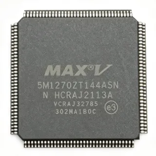
EPM570T144C3N - 570 LEs MAX II CPLD, TQFP-144 | Altera/Intel
MPN: EPM570T144C3N ✓ Active| Qty | Unit Price | Extended |
|---|---|---|
| 1 | $15.6 | $15.60 |
| 10 | $14.25 | $142.50 |
| 100 | $12.4 | $1,240.00 |
| 500 | $10.85 | $5,425.00 |
| 1,000 | $9.6 | $9,600.00 |
Drop-in alternatives for EPM570T144C3N — same package, pin-to-pin compatible. Different-package parts requiring PCB rework are excluded.
Quick Comparison Tool — Select alternative parts for side-by-side comparison:
EPM570GT144C3N
✅ Drop-In✓ In Stock
$28.95 / Unit
View Datasheet →EPM570T144C3
✅ Drop-In✓ In Stock
$27.4 / Unit
View Datasheet →EPM570T144-5
✅ Drop-In✓ In Stock
$9.85 / Unit
View Datasheet →EPM570T144A5N
✅ Drop-In✓ In Stock
$22.8 / Unit
View Datasheet →EPM570T144C5N
✅ Drop-In✓ In Stock
$9.35 / Unit
View Datasheet →EPM570GT144C5N
✅ Drop-In✓ In Stock
$14.2 / Unit
View Datasheet →EPM570T144C3N Maximum Ratings & Electrical Characteristics
| Family | MAX II |
| Device | EPM570 |
| Logic Elements | 570 |
| Typical Macrocells | 440 |
| User I/Os | 116 |
| User Flash Memory (UFM) | 8 Kbits |
| Propagation Delay (tPD) | 5.4 ns (max) |
| Maximum Frequency (fMAX) | 300 MHz (typ) |
| Core Voltage | 3.3 V |
| Operating Temperature | 0C to +85C (commercial) |
| Package | TQFP-144 |
| Process | 0.18 µm, 6-layer-metal flash CMOS |
| Programming Interface | JTAG (IEEE 1149.1), ISP |
| Mounting Type | Surface Mount |
| RoHS Status | Compliant |
EPM570T144C3N Pin Configuration
| Pin 1 | I/O — General-purpose user I/O bank 1 |
| Pin 2 | I/O — General-purpose user I/O bank 1 |
| Pin 3 | I/O — General-purpose user I/O bank 1 |
| Pin 4 | I/O — General-purpose user I/O bank 1 |
| Pin 5 | I/O — General-purpose user I/O bank 1 |
| Pin 6 | I/O — General-purpose user I/O bank 1 |
| Pin 7 | I/O — General-purpose user I/O bank 1 |
| Pin 8 | I/O — General-purpose user I/O bank 1 |
| Pin 9 | I/O — General-purpose user I/O bank 1 |
| Pin 10 | I/O — General-purpose user I/O bank 1 |
| Pin 11 | I/O — General-purpose user I/O bank 1 |
| Pin 12 | I/O — General-purpose user I/O bank 1 |
| Pin 13 | GND — Ground |
| Pin 14 | I/O — General-purpose user I/O bank 1 |
| Pin 15 | I/O — General-purpose user I/O bank 1 |
| Pin 16 | I/O — General-purpose user I/O bank 1 |
| Pin 17 | I/O — General-purpose user I/O bank 1 |
| Pin 18 | I/O — General-purpose user I/O bank 1 |
| Pin 19 | I/O — General-purpose user I/O bank 1 |
| Pin 20 | I/O — General-purpose user I/O bank 1 |
| Pin 21 | I/O — General-purpose user I/O bank 1 |
| Pin 22 | I/O — General-purpose user I/O bank 1 |
| Pin 23 | I/O — General-purpose user I/O bank 1 |
| Pin 24 | I/O — General-purpose user I/O bank 1 |
| Pin 25 | VCCIO1 — I/O bank 1 supply voltage |
| Pin 26 | I/O — General-purpose user I/O bank 1 |
| Pin 27 | I/O — General-purpose user I/O bank 1 |
| Pin 28 | I/O — General-purpose user I/O bank 1 |
| Pin 29 | I/O — General-purpose user I/O bank 1 |
| Pin 30 | I/O — General-purpose user I/O bank 1 |
| Pin 31 | I/O — General-purpose user I/O bank 1 |
| Pin 32 | I/O — General-purpose user I/O bank 1 |
| Pin 33 | I/O — General-purpose user I/O bank 1 |
| Pin 34 | I/O — General-purpose user I/O bank 1 |
| Pin 35 | I/O — General-purpose user I/O bank 1 |
| Pin 36 | I/O — General-purpose user I/O bank 1 |
| Pin 37 | GND — Ground |
| Pin 38 | I/O — General-purpose user I/O bank 2 |
| Pin 39 | I/O — General-purpose user I/O bank 2 |
| Pin 40 | I/O — General-purpose user I/O bank 2 |
| Pin 41 | I/O — General-purpose user I/O bank 2 |
| Pin 42 | I/O — General-purpose user I/O bank 2 |
| Pin 43 | I/O — General-purpose user I/O bank 2 |
| Pin 44 | I/O — General-purpose user I/O bank 2 |
| Pin 45 | I/O — General-purpose user I/O bank 2 |
| Pin 46 | I/O — General-purpose user I/O bank 2 |
| Pin 47 | I/O — General-purpose user I/O bank 2 |
| Pin 48 | I/O — General-purpose user I/O bank 2 |
| Pin 49 | I/O — General-purpose user I/O bank 2 |
| Pin 50 | VCCIO2 — I/O bank 2 supply voltage |
| Pin 51 | I/O — General-purpose user I/O bank 2 |
| Pin 52 | I/O — General-purpose user I/O bank 2 |
| Pin 53 | I/O — General-purpose user I/O bank 2 |
| Pin 54 | I/O — General-purpose user I/O bank 2 |
| Pin 55 | I/O — General-purpose user I/O bank 2 |
| Pin 56 | I/O — General-purpose user I/O bank 2 |
| Pin 57 | I/O — General-purpose user I/O bank 2 |
| Pin 58 | I/O — General-purpose user I/O bank 2 |
| Pin 59 | I/O — General-purpose user I/O bank 2 |
| Pin 60 | I/O — General-purpose user I/O bank 2 |
| Pin 61 | I/O — General-purpose user I/O bank 2 |
| Pin 62 | GND — Ground |
| Pin 63 | I/O — General-purpose user I/O bank 3 |
| Pin 64 | I/O — General-purpose user I/O bank 3 |
| Pin 65 | I/O — General-purpose user I/O bank 3 |
| Pin 66 | I/O — General-purpose user I/O bank 3 |
| Pin 67 | I/O — General-purpose user I/O bank 3 |
| Pin 68 | I/O — General-purpose user I/O bank 3 |
| Pin 69 | I/O — General-purpose user I/O bank 3 |
| Pin 70 | I/O — General-purpose user I/O bank 3 |
| Pin 71 | I/O — General-purpose user I/O bank 3 |
| Pin 72 | I/O — General-purpose user I/O bank 3 |
| Pin 73 | I/O — General-purpose user I/O bank 3 |
| Pin 74 | I/O — General-purpose user I/O bank 3 |
| Pin 75 | VCCIO3 — I/O bank 3 supply voltage |
| Pin 76 | I/O — General-purpose user I/O bank 3 |
| Pin 77 | I/O — General-purpose user I/O bank 3 |
| Pin 78 | I/O — General-purpose user I/O bank 3 |
| Pin 79 | I/O — General-purpose user I/O bank 3 |
| Pin 80 | I/O — General-purpose user I/O bank 3 |
| Pin 81 | I/O — General-purpose user I/O bank 3 |
| Pin 82 | I/O — General-purpose user I/O bank 3 |
| Pin 83 | I/O — General-purpose user I/O bank 3 |
| Pin 84 | I/O — General-purpose user I/O bank 3 |
| Pin 85 | I/O — General-purpose user I/O bank 3 |
| Pin 86 | I/O — General-purpose user I/O bank 3 |
| Pin 87 | GND — Ground |
| Pin 88 | I/O — General-purpose user I/O bank 4 |
| Pin 89 | I/O — General-purpose user I/O bank 4 |
| Pin 90 | I/O — General-purpose user I/O bank 4 |
| Pin 91 | I/O — General-purpose user I/O bank 4 |
| Pin 92 | I/O — General-purpose user I/O bank 4 |
| Pin 93 | I/O — General-purpose user I/O bank 4 |
| Pin 94 | I/O — General-purpose user I/O bank 4 |
| Pin 95 | I/O — General-purpose user I/O bank 4 |
| Pin 96 | I/O — General-purpose user I/O bank 4 |
| Pin 97 | I/O — General-purpose user I/O bank 4 |
| Pin 98 | I/O — General-purpose user I/O bank 4 |
| Pin 99 | I/O — General-purpose user I/O bank 4 |
| Pin 100 | VCCIO4 — I/O bank 4 supply voltage |
| Pin 101 | I/O — General-purpose user I/O bank 4 |
| Pin 102 | I/O — General-purpose user I/O bank 4 |
| Pin 103 | I/O — General-purpose user I/O bank 4 |
| Pin 104 | I/O — General-purpose user I/O bank 4 |
| Pin 105 | I/O — General-purpose user I/O bank 4 |
| Pin 106 | I/O — General-purpose user I/O bank 4 |
| Pin 107 | I/O — General-purpose user I/O bank 4 |
| Pin 108 | I/O — General-purpose user I/O bank 4 |
| Pin 109 | I/O — General-purpose user I/O bank 4 |
| Pin 110 | I/O — General-purpose user I/O bank 4 |
| Pin 111 | I/O — General-purpose user I/O bank 4 |
| Pin 112 | GND — Ground |
| Pin 113 | TDI — JTAG Test Data In |
| Pin 114 | TMS — JTAG Test Mode Select |
| Pin 115 | TCK — JTAG Test Clock |
| Pin 116 | TDO — JTAG Test Data Out |
| Pin 117 | VCCINT — Core supply voltage (3.3V) |
| Pin 118 | nSTATUS — Configuration status (open-drain) |
| Pin 119 | CONF_DONE — Configuration done (open-drain) |
| Pin 120 | nCONFIG — Configuration start (active-low) |
| Pin 121 | MSEL0 — Configuration mode select 0 |
| Pin 122 | MSEL1 — Configuration mode select 1 |
| Pin 123 | MSEL2 — Configuration mode select 2 |
| Pin 124 | GND — Ground |
| Pin 125 | I/O — General-purpose user I/O bank 5 |
| Pin 126 | I/O — General-purpose user I/O bank 5 |
| Pin 127 | I/O — General-purpose user I/O bank 5 |
| Pin 128 | I/O — General-purpose user I/O bank 5 |
| Pin 129 | I/O — General-purpose user I/O bank 5 |
| Pin 130 | I/O — General-purpose user I/O bank 5 |
| Pin 131 | I/O — General-purpose user I/O bank 5 |
| Pin 132 | VCCIO5 — I/O bank 5 supply voltage |
| Pin 133 | I/O — General-purpose user I/O bank 5 |
| Pin 134 | I/O — General-purpose user I/O bank 5 |
| Pin 135 | I/O — General-purpose user I/O bank 5 |
| Pin 136 | I/O — General-purpose user I/O bank 5 |
| Pin 137 | I/O — General-purpose user I/O bank 5 |
| Pin 138 | I/O — General-purpose user I/O bank 5 |
| Pin 139 | I/O — General-purpose user I/O bank 5 |
| Pin 140 | I/O — General-purpose user I/O bank 5 |
| Pin 141 | I/O — General-purpose user I/O bank 5 |
| Pin 142 | GND — Ground |
| Pin 143 | I/O — General-purpose user I/O bank 5 |
| Pin 144 | I/O — General-purpose user I/O bank 5 |
Safe Operating Area (SOA) & Thermal Characteristics
No official SOA curve available for this digital IC. Always operate within absolute maximum ratings specified in the datasheet. Ensure adequate cooling and derate as needed.
Typical Applications
EPM570T144C3N is suitable for 6 applications: Industrial Control Glue Logic, Communications Infrastructure I/O Bridging, Automotive Body Electronics, Microcontroller Expansion and Voltage Translation, Consumer Electronics Glue Logic, Prototyping and Rapid Design Iteration.
Industrial Control Glue Logic
The EPM570T144C3N is widely used as glue logic on industrial control boards where 116 user I/Os and 570 LEs provide ample capacity for I/O expansion and bus decode. Its 5.4 ns pin-to-pin propagation delay and ~300 MHz maximum frequency suit interrupt steering and high-speed register decoding between microcontrollers and peripherals. The 3.3V core and MultiVolt I/O support bridging to 1.5V, 1.8V, 2.5V, and 3.3V rails without external level shifters. The flash-based non-volatile configuration means the device is functional microseconds after power-up - ideal for factory-automation controllers that must respond deterministically the moment VCC stabilizes. JTAG-ISP enables field firmware updates.
Recommended
Communications Infrastructure I/O Bridging
In routers, switches, and base-station line cards, the EPM570T144C3N bridges between ASIC/FPGA banks and backplane connectors operating at multiple voltage standards. The 116 user I/Os spread across the TQFP-144 footprint accommodate the high pin count needed for parallel bus expansion, while the LVCMOS/LVTTL/PCI/SSTL I/O standards supported by MultiVolt cover legacy 5V-tolerant interfaces. The 8 Kbit User Flash Memory block can store board revision IDs or boot-time configuration constants. With 5.4 ns tPD, the device introduces minimal latency in address decode and chip-select paths feeding the main processor.
Recommended
Automotive Body Electronics
Although the EPM570T144C3N is commercial-temperature (0C to +85C), its MAX II architecture is also widely deployed on automotive body and infotainment boards for non-safety functions such as LED driving control, button matrix scanning, and CAN/LIN signal conditioning. The 5.4 ns propagation delay supports real-time LED PWM and button de-bounce logic. The 8 Kbit UFM can store calibration tables or board-identifying data. For under-hood or safety-critical automotive functions, engineers should migrate to the AEC-Q100 qualified MAX V family - but for body and infotainment the EPM570T144C3N remains a cost-effective, proven solution in volume production.
Recommended
Microcontroller Expansion and Voltage Translation
The EPM570T144C3N is a classic choice for expanding a microcontroller's limited I/O count into 116 general-purpose pins while translating voltage levels between incompatible rails. MultiVolt I/O allow direct interfacing between a 1.8V MCU and 3.3V peripherals without external level shifters. With 570 LEs and 8 Kbit UFM, designers can implement protocol bridges, state machines, and timing-sensitive interfaces that would otherwise consume excessive MCU cycles. JTAG-ISP allows field firmware updates after the MCU has booted, supporting late-stage customization and factory provisioning.
Recommended
Consumer Electronics Glue Logic
Replacing dozens of discrete 74-series logic chips, the EPM570T144C3N consolidates glue logic on consumer motherboards, set-top boxes, and display controllers. Its instant-on non-volatile configuration eliminates the boot-time latency that discrete PLDs and small FPGAs impose, enabling immediate response to user input. The 5.4 ns tPD supports high-speed interfaces such as LVDS signaling and parallel RGB routing, while the 116 user I/Os accommodate multiple connector pinouts. Quartus design entry and JTAG programming shorten development cycles and enable rapid board spin revisions.
Recommended
Prototyping and Rapid Design Iteration
Designers prototyping new board designs favor the EPM570T144C3N because its Quartus design flow, JTAG in-system programmability, and instant-on behavior allow rapid hardware/software co-design iteration. Design changes can be downloaded in seconds via the JTAG header without removing the device or reprogramming a boot PROM. The 570 LEs and 8 Kbit UFM provide generous headroom for late-stage feature additions, and the TQFP-144 package is hand-solderable for low-volume prototyping. Once the design stabilizes, the same Quartus bitstream can be programmed into higher-density MAX II variants (EPM1270, EPM2210) without code changes.
Recommended
Recommended Products Summary
Engineering reference data for EPM570T144C3N — comparison, design guidance, and compliance information.
Selection Guide
Comparison with Alternatives
| Parameter | This Product | EPM570GT144C3N | EPM570T144C3 | EPM570T144-5 | EPM570T144A5N | EPM570T144C5N |
|---|---|---|---|---|---|---|
| Brand | Altera (now Intel) | Altera (now Intel) | Altera (now Intel) | Altera (now Intel) | Altera (now Intel) | Altera (now Intel) |
| Package | TQFP-144 | TQFP-144 - same | TQFP-144 - same | TQFP-144 - same | TQFP-144 - same | TQFP-144 - same |
| Logic Elements | 570 | 570 | 570 | 570 | 570 | 570 |
| Macrocells (typical) | 440 | 440 | 440 | 440 | 440 | 440 |
| User I/Os | 116 | 116 | 116 | 116 | 116 | 116 |
| tPD (max) | 5.4 ns | 5.4 ns | 5.4 ns | ~7.0 ns | ~8.0 ns | ~7.0 ns |
| Speed Grade | C3 | C3 | C3 | -5 | A5 | C5 |
| Core Voltage | 3.3 V | 3.3 V | 3.3 V | 3.3 V | 3.3 V | 3.3 V |
Key Differentiators
- C3 speed grade is the fastest commercial option (vs EPM570T144C5N)
- TQFP-144 footprint exposes 116 user I/Os (vs EPM570T100C5N)
- Non-volatile instant-on configuration (vs Small SRAM-based FPGAs)
Design Notes
Estimated: the EPM570T144C3N core draws approximately 30-50 mA quiescent plus dynamic current proportional to switching frequency. Place a 100 nF decoupling capacitor within 5 mm of every VCCINT and VCCIOx pin, plus a single 10 uF bulk tantalum or ceramic on each supply rail. TQFP-144 packages have multiple GND pins - connect all of them to a low-impedance ground plane for clean switching returns and reduced EMI. Avoid splitting the ground plane under the device to preserve signal integrity.
Route JTAG signals (TDI, TMS, TCK, TDO) as a daisy chain if multiple devices share the bus, with a 4.7 kohm pull-up on TCK and TMS per IEEE 1149.1 recommendations. Keep JTAG traces short and isolated from high-speed switching I/O to avoid programming failures. For 116 simultaneous switching outputs, use controlled-impedance traces and matched series termination to minimize reflections; refer to AN 224 (Altera) for high-speed PCB design guidelines.
Do not leave MSEL pins floating - strap them to defined logic levels per the MAX II handbook configuration mode table for the desired programming mode. The nCONFIG, nSTATUS, and CONF_DONE pins are open-drain and require external pull-ups; omitting these pull-ups prevents the device from entering user mode at power-up. The 8 Kbit UFM block has a finite endurance (~1000 cycles) and ~20-year data retention - verify these limits against your programming volume and field-life requirements.
Compliance Information
RoHS compliant per Altera/Intel product page. Commercial temperature grade only - not AEC-Q100 qualified; for automotive safety-critical applications use MAX V family.