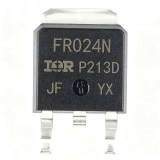
IRLR3110ZTRLPBF - 100V 63A N-Channel HEXFET MOSFET | Infineon
MPN: IRLR3110ZTRLPBF ✓ Active| Qty | Unit Price | Extended |
|---|---|---|
| 1 | $1.42 | $1.42 |
| 10 | $1.18 | $11.80 |
| 100 | $0.94 | $94.00 |
| 500 | $0.78 | $390.00 |
| 1,000 | $0.65 | $650.00 |
IRLR3110ZTRLPBF Overview
An N-channel power MOSFET is a voltage-controlled semiconductor switch whose drain current is modulated by a gate-source voltage. The HEXFET family refers to Infineon/IInternational Rectifier's vertically-diffused trench MOSFET architecture, which sits in the broader power MOSFET category within discrete semiconductors. These devices are used as switching elements or low-resistance pass elements in power conversion systems, where their low RDS(on) minimizes conduction loss and their high-speed switching capability reduces switching loss.
Key specifications include VDS max of 100 V, RDS(on) max of 14 mΩ (or 11 mΩ per third-party listings), continuous drain current up to 42 A at TC and pulsed drain current rating supporting the 63 A ID max figure at lower temperature conditions, with gate charge of 34 nC. The logic-level gate drive simplifies interfacing directly to microcontrollers, gate drivers, and PWM controllers without requiring a separate charge-pump or bootstrap supply.
The TO-252AA (DPAK) package offers a low thermal-resistance path through the tab, with the part rated at 140 W power dissipation at TC. The exposed tab functions as the drain connection, while gate, drain, and source are arranged in the standard DPAK pinout. Repetitive-avalanche-rated cells and 175°C junction operation make this part suitable for rugged industrial environments with high inrush or unclamped inductive switching.
Typical applications include DC-DC converters in industrial 48 V bus systems, motor drive H-bridges for 24-72 V brushless DC motors, solenoid and relay drivers, power OR-ing, battery protection circuits, and primary-side switching for telecom bricks. Its logic-level gate and low RDS(on) also make it appropriate for hot-swap controllers and electronic fuse implementations.
When designing with this part, place the gate driver as close as possible to the gate pin and use a 10 kΩ pull-down on the gate to prevent false turn-on during power-up. Ensure the tab thermal pad carries at least 1 square inch of copper pour, and verify SOA against worst-case VDS and ID combinations before finalizing the design.
This page synthesizes distributor pricing, parametrically validated drop-in alternatives, and practical design notes not found in a single manufacturer datasheet or distributor listing.
Drop-in alternatives for IRLR3110ZTRLPBF — same package, pin-to-pin compatible. Different-package parts requiring PCB rework are excluded.
Variants in this series
Same-series models that are drop-in compatible with IRLR3110ZTRLPBF (same form factor and footprint) — differing in RoHS Status, Technology.
Quick Comparison Tool — Select alternative parts for side-by-side comparison:
IRLR3110ZTRPBF
✅ Drop-In✓ In Stock
$0.66 / Unit
View Datasheet →IRLR3110ZPBF
✅ Drop-In📋 Reference alternative (not in catalog)
AUIRLR3110ZTRL
✅ Drop-In📋 Reference alternative (not in catalog)
IRLR3110ZTRLPBF Maximum Ratings & Electrical Characteristics
| Transistor Polarity | N-Channel |
| Drain-Source Voltage (VDS) | 100 V |
| Continuous Drain Current (ID) at TC | 42 A |
| Maximum Drain Current (ID max) | 63 A |
| On-Resistance (RDS(on) max) | 14 mOhm |
| Gate Charge (Qg) | 34 nC |
| Technology | IR HEXFET / Trench MOSFET |
| Gate Drive Level | Logic-Level |
| Power Dissipation (PD) at TC | 140 W |
| Operating Junction Temperature | -55C to +175C |
| Package | TO-252AA (DPAK) |
| Mounting Type | Surface Mount |
| Pin Count | 3 (Drain, Gate, Source + Tab) |
| Repetitive Avalanche Rated | Yes |
| RoHS Status | Compliant (PBF suffix) |
IRLR3110ZTRLPBF Pin Configuration
| Pin 1 | Gate — Logic-level gate input for MOSFET control |
| Pin 2 | Drain — Power drain connection (also connected to tab) |
| Pin 3 | Source — Power source / return path |
| Pin Tab | Drain (Tab) — Exposed drain tab for electrical contact and thermal dissipation |
Safe Operating Area (DC) - DPAK on 1 sq inch copper pour
Typical Applications
IRLR3110ZTRLPBF is suitable for 6 applications: Industrial 48V DC-DC Converters, Brushless DC Motor Drive H-Bridges, Solenoid and Relay Driver Circuits, Battery Protection and Power OR-ing, Telecom Brick Primary-Side Switching, Hot-Swap and Electronic Fuse Circuits.
Industrial 48V DC-DC Converters
The IRLR3110ZTRLPBF is well-suited for primary-side switching in 48 V nominal industrial DC-DC converters stepping down to 12 V, 5 V, or 3.3 V logic rails. With VDS max of 100 V, the part provides comfortable headroom above the 48 V bus plus transients, while its 14 mΩ RDS(on) minimizes conduction loss at the high currents encountered in such converters. Placed on the low-side of a synchronous buck topology, the device's logic-level gate drive allows direct control from a 5 V or 3.3 V PWM controller without an additional gate-driver supply. The 175°C junction rating and repetitive-avalanche capability handle the high di/dt and unclamped energy events typical during output short or inductor saturation faults. Pair with companion gate drivers and controller ICs listed below.
Recommended
Brushless DC Motor Drive H-Bridges
In 24-72 V brushless DC motor drives, the IRLR3110ZTRLPBF can be used as the low-side or high-side switching element in a three-phase H-bridge. The 42 A continuous drain current (63 A pulsed) easily drives mid-power industrial motors in the 1-3 kW range, while the logic-level gate input simplifies interfacing to 3.3 V MCUs. The repetitive-avalanche rating protects the device during regenerative braking events when back-EMF drives the drain above VDS max momentarily. Thermal management via the DPAK tab allows sustained high current without additional heatsinking in well-designed copper pours. Combine with companion gate drivers and position-sensing ICs for a complete motor-control solution.
Recommended
Solenoid and Relay Driver Circuits
The IRLR3110ZTRLPBF is ideal for driving inductive loads such as 24 V or 48 V solenoids, relays, and contactors in industrial automation systems. The low RDS(on) of 14 mΩ means low-side switching dissipation is minimal even at the high inrush currents encountered when energizing large coils. Built-in repetitive avalanche rating protects the device during flyback events when the solenoid is de-energized without an external freewheeling diode. Logic-level gate drive allows direct switching from PLC outputs or microcontroller GPIOs without additional driver stages. The DPAK package's small footprint simplifies integration into multi-channel driver boards.
Recommended
Battery Protection and Power OR-ing
The IRLR3110ZTRLPBF serves as a reverse-battery protection or power OR-ing MOSFET in 24-48 V battery-backed systems. Used as a low-side disconnect switch, its low RDS(on) keeps voltage drop minimal during normal operation, preserving efficiency. The 100 V VDS rating easily exceeds the typical 36-60 V battery voltages plus inductive transients when cables are hot-plugged. Logic-level gate drive simplifies control from battery-management ICs operating from 3.3 V or 5 V rails. The repetitive-avalanche rating protects against load-dump events in automotive or industrial 24 V truck systems. Pair with battery monitor ICs for complete protection.
Recommended
Telecom Brick Primary-Side Switching
In isolated telecom DC-DC converters operating from 36-72 V input bus, the IRLR3110ZTRLPBF can be used on the primary side of a full-bridge or push-pull topology. The 100 V VDS rating provides adequate margin above 72 V input plus reflected secondary voltage and leakage spikes. Low RDS(on) reduces conduction loss during the high-current primary cycles typical of 1-3 kW brick converters. Logic-level gate drive simplifies interfacing to digital controllers that operate from 3.3 V. Repetitive-avalanche rating handles the energy stored in the transformer leakage inductance at turn-off. The DPAK footprint eases high-density PCB layout.
Recommended
Hot-Swap and Electronic Fuse Circuits
The IRLR3110ZTRLPBF functions as the series pass element in 24-48 V hot-swap controllers and electronic fuse circuits, where its low RDS(on) minimizes voltage drop across the protection path. The logic-level gate enables closed-loop control with a hot-swap controller IC, allowing inrush current limiting and circuit-breaker behavior. The 100 V VDS rating supports 48 V nominal systems with margin for transients. The repetitive-avalanche rating protects the device during sudden load-dump events when the load is disconnected abruptly. The DPAK package's exposed tab provides efficient heat removal for sustained high current.
Recommended
Recommended Products Summary
Engineering reference data for IRLR3110ZTRLPBF — comparison, design guidance, and compliance information.
Selection Guide
Comparison with Alternatives
| Parameter | This Product | IRLR3110ZTRPBF | IRLR3110ZPBF | AUIRLR3110ZTRL |
|---|---|---|---|---|
| Brand | Infineon | Infineon | Infineon | Infineon |
| Package | TO-252AA (DPAK) | TO-252AA (DPAK) | TO-252AA (DPAK) | TO-252AA (DPAK) |
| Drain-Source Voltage (VDS) | 100 V | 100 V | 100 V | 100 V |
| Continuous Drain Current at TC | 42 A | 42 A | 42 A | 42 A |
| Maximum Drain Current | 63 A | 63 A | 63 A | 63 A |
| On-Resistance RDS(on) max | 14 mOhm | 14 mOhm | 14 mOhm | 14 mOhm |
| Gate Charge Qg | 34 nC | 34 nC | 34 nC | 34 nC |
| Automotive Qualified | No | No | No | Yes (AEC-Q101) |
| Tape and Reel Orientation | Left | Standard | N/A (Tube) | Standard |
Key Differentiators
- Logic-level gate drive for direct microcontroller interfacing (vs IRFB4110PBF (10V gate drive required))
- Lower on-resistance per silicon area via IR HEXFET trench technology (vs Standard planar MOSFETs in same package)
- Repetitive avalanche rated for unclamped inductive switching (vs Standard MOSFETs without avalanche rating)
- 175°C maximum junction temperature for industrial thermal margin (vs Standard 150°C rated MOSFETs)
Design Notes
Estimated: With TC held at 25C and 1 square inch of copper pour, the DPAK package theta_JA is approximately 50 C/W. At full 42 A continuous current with VIN = 50 V and VOUT = 0 V (worst case), dissipation approaches the 140 W limit. For sustained high-current operation, derate the part to keep junction below 150C. Use multiple thermal vias under the tab to a bottom-side copper plane for improved heat transfer. At a more realistic 5W dissipation (typical switching application), the part operates safely at 25C ambient.
Place the gate drive trace as short and direct as possible, with a 10 kΩ pull-down resistor from gate to source to prevent unintended turn-on during power-up or transient events. Keep the high-current drain and source loops minimal to reduce parasitic inductance that can cause voltage overshoot exceeding VDS max during switching. The exposed tab must be soldered to a copper pad of at least 80 mm² for proper thermal dissipation and electrical connection.
Do not exceed VDS max of 100 V - inductive load switching without proper snubbing can easily exceed this rating during turn-off. Verify SOA against worst-case continuous and pulsed conditions before deployment. The logic-level gate requires VGS of at least 4.5 V for full enhancement; lower gate voltages result in partial turn-on and dramatically higher RDS(on). Always check avalanche energy (EAS) rating when switching inductive loads without freewheeling diodes.
For double-sided PCBs, place thermal vias in a 3x3 grid pattern under the DPAK tab, each via approximately 0.3 mm diameter with 0.05 mm plating. Connect the via farm to a bottom-side copper pour that extends at least 100 mm². Avoid routing high-current traces directly under the package to prevent solder joint stress during thermal cycling. Use a land pattern compliant with IPC-7351 nominal DPAK dimensions for manufacturability.
Compliance Information
RoHS and REACH compliant per PBF suffix in MPN. Standard part is not AEC-Q100 qualified; choose AUIRLR3110ZTRL for AEC-Q101 automotive qualification. Lead-free reflow compatible per JESD22-A111.