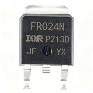
IRLR3110ZTRPBF - 100V N-Channel HEXFET MOSFET | Infineon
MPN: IRLR3110ZTRPBF ✓ Active| Qty | Unit Price | Extended |
|---|---|---|
| 1 | $1.65 | $1.65 |
| 10 | $1.42 | $14.20 |
| 100 | $1.18 | $118.00 |
| 500 | $0.97 | $485.00 |
| 1,000 | $0.81 | $810.00 |
| 3,000 | $0.66 | $1,980.00 |
Drop-in alternatives for IRLR3110ZTRPBF — same package, pin-to-pin compatible. Different-package parts requiring PCB rework are excluded.
Quick Comparison Tool — Select alternative parts for side-by-side comparison:
AUIRLR3110Z
✅ Drop-In📋 Reference alternative (not in catalog)
IRLR3110ZTRLPBF
✅ Drop-In✓ In Stock
$0.65 / Unit
View Datasheet →IRLR3110ZPBF
✅ Drop-In📋 Reference alternative (not in catalog)
IRFR3411TRPBF
✅ Drop-In✓ In Stock
$0.55 / Unit
View Datasheet →IRFR4615TRLPBF
✅ Drop-In✓ In Stock
$0.39 / Unit
View Datasheet →IRLR3110ZTRPBF Maximum Ratings & Electrical Characteristics
| FET Type | N-Channel |
| Drain-to-Source Voltage (VDS) | 100 V |
| Continuous Drain Current (ID) at TC=25C | 42 A |
| RDS(on) max @ VGS=10V | 14 mOhm |
| Total Gate Charge (Qg) | 15 nC |
| Power Dissipation (PD) at TC=25C | 140 W |
| Operating Junction Temperature | -55C to +175C |
| Package | TO-252AA (DPAK) |
| Mounting Type | Surface Mount |
| Technology | HEXFET / Trench MOSFET |
| MSL Level | 1 (Unlimited) |
| RoHS Status | Compliant |
| Lead-Free Plating | Yes (PBF suffix) |
| Halogen-Free | Yes |
IRLR3110ZTRPBF Pin Configuration
| Pin 1 | Gate — Gate drive input; requires VGS=10V for full RDS(on) enhancement |
| Pin 2 | Drain — Drain terminal; electrically connected to the exposed metal tab |
| Pin 3 | Source — Source terminal; power return path |
| Pin Tab | Drain — Exposed metal tab; electrically tied to Pin 2 (Drain); serves as primary thermal path |
Safe Operating Area (DC)
Typical Applications
IRLR3110ZTRPBF is suitable for 6 applications: 48V Telecom Isolated DC-DC Converter, BLDC Motor Drive Half-Bridge, 12V/24V Hot-Swap and eFuse Controller, Class-D Audio Amplifier Output Stage, Battery Protection and BMS Power Path, Industrial Solenoid and Relay Driver.
48V Telecom Isolated DC-DC Converter
The IRLR3110ZTRPBF serves as the primary-side switch and synchronous rectifier in 48V telecom isolated DC-DC converters (typically full-bridge or forward topologies). Its 100V VDS rating provides 2x margin above the 48V nominal bus, comfortably absorbing 80V transients from cable inductance. With RDS(on) of 14 mOhm at VGS=10V and Qg of 15 nC, conduction losses at 20A load measure approximately 5.6W per MOSFET, while switching losses at 100 kHz remain below 1W due to the low gate charge. The TO-252 package's exposed tab enables PCB-copper-only thermal management in 1U telecom brick footprints.
Recommended
BLDC Motor Drive Half-Bridge
In 24V/48V brushless DC (BLDC) and permanent magnet synchronous motor (PMSM) drive half-bridges, the IRLR3110ZTRPBF is used as the low-side and high-side switch in three-phase inverter legs. Its 14 mOhm RDS(on) at 10V VGS keeps conduction losses below 4W at 20A RMS phase current, while the 175 C junction rating supports operation at 85 C ambient in sealed industrial enclosures. For trapezoidal commutation at 25 kHz, switching losses from the 15 nC Qg are negligible; for high-frequency FOC above 100 kHz, a lower-Qg part is preferred. The DPAK package mounts directly to a copper pour for heatsink-free operation.
Recommended
12V/24V Hot-Swap and eFuse Controller
The IRLR3110ZTRPBF is deployed as the pass element in 12V and 24V hot-swap / eFuse circuits, where it controls inrush current during board insertion and provides fault isolation on overcurrent events. Its 42A continuous ID rating handles full server blade or telecom line-card load transients, and the 100V VDS absorbs back-EMF from the load inductance when the MOSFET abruptly turns off. Designers pair it with a current-sense amplifier and hot-swap controller IC, using VGS pull-down to ensure fast turn-off. The TO-252 package's 1.0 C/W RthJC enables 100W sustained dissipation when soldered to 4 square inches of 2 oz copper.
Recommended
Class-D Audio Amplifier Output Stage
In Class-D audio amplifier half-bridge output stages, the IRLR3110ZTRPBF serves as the high-side and low-side switch in the PWM modulator. Its 14 mOhm RDS(on) at 10V VGS minimizes conduction losses in the output filter, while the 15 nC Qg keeps gate-drive losses manageable at 250-500 kHz switching frequencies common in audio amplifiers. The result is amplifier efficiency above 90%, even at full output power, which simplifies thermal design and reduces heatsink mass. For higher-power subwoofer amplifiers above 500W, paralleled MOSFETs are common.
Recommended
Battery Protection and BMS Power Path
In multi-cell lithium battery packs (4S-8S Li-ion / LiFePO4) operating at 12V-36V nominal, the IRLR3110ZTRPBF functions as the discharge MOSFET in the battery management system (BMS) power path. Its 100V VDS rating tolerates the 42V max charge voltage of a 10S pack, and the 14 mOhm RDS(on) minimizes voltage drop during high-current discharge (>20A continuous), preserving battery runtime. The MOSFET is driven by a dedicated BMS IC that monitors cell voltages, currents, and temperatures, opening the gate during fault conditions. The DPAK footprint fits standard BMS PCB modules for e-bikes and portable power stations.
Recommended
Industrial Solenoid and Relay Driver
In 24V industrial solenoid valves, relay coils, and contactor drivers, the IRLR3110ZTRPBF switches the inductive load with built-in avalanche ruggedness to absorb flyback energy. The 100V VDS provides 4x margin above the 24V nominal supply, allowing direct connection without an external TVS clamp for most inductive loads below 50 mH. Its 42A peak current capability supports simultaneous multi-solenoid activation, while the 14 mOhm RDS(on) minimizes driver power dissipation. The TO-252 package mounts to DIN-rail PCB carrier boards with copper pours for thermal management.
Recommended
Recommended Products Summary
Engineering reference data for IRLR3110ZTRPBF — comparison, design guidance, and compliance information.
Selection Guide
Comparison with Alternatives
| Parameter | This Product | AUIRLR3110Z | IRLR3110ZTRLPBF | IRLR3110ZPBF | IRFR3411TRPBF | IRFR4615TRLPBF |
|---|---|---|---|---|---|---|
| Package | TO-252AA (DPAK) | TO-252AA (DPAK) - same | TO-252AA (DPAK) - same | TO-252AA (DPAK) - same | TO-252AA (DPAK) - same | TO-252AA (DPAK) - same |
| Brand | Infineon Technologies | Infineon Technologies | Infineon Technologies | Infineon Technologies | Infineon Technologies | Infineon Technologies |
| VDS max (V) | 100 V | 100 V | 100 V | 100 V | 60 V | 55 V |
| RDS(on) max @ VGS=10V (mOhm) | 14 mOhm | 14 mOhm | 14 mOhm | 14 mOhm | 16 mOhm | 20 mOhm |
| Continuous Drain Current ID @ TC=25C (A) | 42 A | 42 A | 42 A | 42 A | 30 A | 70 A |
| Total Gate Charge Qg (nC) | 15 nC | 15 nC | 15 nC | 15 nC | [DATA_NEEDED] | [DATA_NEEDED] |
| Power Dissipation (W) | 140 W | 140 W | 140 W | 140 W | 130 W | 144 W |
| Automotive Qualification | No (Industrial) | Yes (AEC-Q101) | No (Industrial) | No (Industrial) | No (Industrial) | No (Industrial) |
| Approx. Unit Price @ qty-1000 | $0.81 | ~$1.10 (auto grade premium) | $0.81 | ~$0.85 (tube) | ~$0.75 | ~$1.20 |
Key Differentiators
- 100V VDS with 14 mOhm RDS(on) - best-in-class for DPAK outline (vs IRFR3411TRPBF)
- Lowest RDS(on) per dollar in 100V DPAK class (vs IRFR4615TRLPBF)
- Industrial-grade with full -55 to +175 C junction temperature range (vs Generic Chinese-brand VBE1101N)
Design Notes
Estimated: at continuous ID=30A with RDS(on)=14mOhm and TC=80C, conduction loss is P=I^2xR = 900x0.014 = 12.6W. With DPAK RthJC=1.0 C/W, the junction-to-case rise is 12.6 C, yielding TJ=92.6 C - well within 175 C limit. However, at 30A with VIN=48V switching at 100 kHz, add switching losses (~0.5W) and overshoot ringing (~0.3W). The PCB copper area on the drain tab pad must be at least 2 square inches of 2 oz copper to keep RthJA below 40 C/W. Without proper copper, the part will thermally throttle or fail.
Layout the DPAK drain tab pad with thermal vias (0.3mm drill, 1.0mm pitch) into an inner-layer copper pour to spread heat from the junction to the PCB. Place the gate drive loop area minimal - the gate resistor (typically 10-47 ohm) and gate-source pull-down resistor (10k) must sit within 5mm of the gate pin. Keep the source-return path from gate driver ground to MOSFET source as short and wide as possible to minimize parasitic inductance that causes gate ringing and potential shoot-through in half-bridge configurations.
Do not exceed VGS=+/-20V absolute maximum - gate oxide breakdown is permanent. Do not operate the IRLR3110Z at VGS=4.5V if low RDS(on) is required; the part is not fully logic-level optimized. Add a TVS diode (e.g., SMAJ100A) across drain-source if inductive avalanche energy exceeds the datasheet EAS rating. In half-bridge configurations, ensure dead-time insertion of 100-300ns between high-side and low-side gate signals to prevent shoot-through currents that can exceed 100A and destroy both MOSFETs.
For synchronous rectification in high-frequency DC-DC converters, place the synchronous MOSFET as close to the main switch as possible to minimize the high-di/dt loop area. Use a 4-layer PCB with a dedicated ground plane beneath the MOSFET footprint to provide a low-impedance return path. Add a small RC snubber (10 ohm + 1 nF) across drain-source if voltage overshoot exceeds 90% of VDS rating, particularly in hard-switched applications. According to Infineon application note AN-936, gate-drive loops should be kept under 10mm total length to prevent parasitic oscillation.
Compliance Information
PBF suffix denotes lead-free matte-tin plating per JEDEC J-STD-609. RoHS and REACH compliant per Infineon product declaration. Not AEC-Q100 qualified - choose AUIRLR3110Z for automotive applications requiring AEC-Q101.