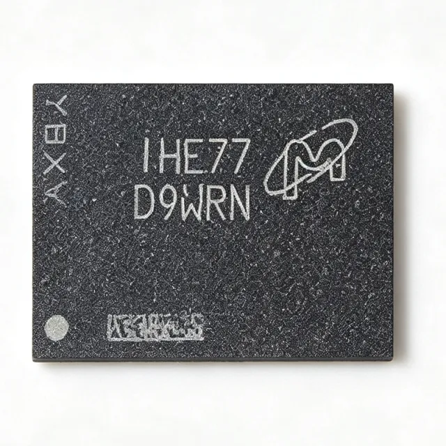
MT53E384M32D2DS-053 WT:E - 12Gbit LPDDR4 SDRAM | Micron
MPN: MT53E384M32D2DS-053 WT:E ✓ Active| Qty | Unit Price | Extended |
|---|---|---|
| 1 | $15.77 | $15.77 |
| 10 | $14.85 | $148.50 |
| 100 | $13.6 | $1,360.00 |
| 500 | $12.45 | $6,225.00 |
| 1,000 | $11.3 | $11,300.00 |
MT53E384M32D2DS-053 WT:E Overview
Mobile LPDDR4 (Low Power Double Data Rate 4) SDRAM is a JEDEC-defined DRAM category optimized for battery-powered systems. Within the memory hierarchy, LPDDR4 sits in the mobile DRAM family alongside LPDDR4X and LPDDR5, descending from LPDDR3 and DDR3L. Compared with desktop DDR SDRAM, LPDDR4 trades absolute peak bandwidth for dramatically lower operating voltage and standby current, making it the dominant main-memory technology in smartphones, tablets, and embedded systems.
Key features of this device include the 12Gbit total density implemented as two stacked 6Gbit die (DDP), a 32-bit data width, and a -053 speed grade corresponding to 1866 Mbps per pin. The WT:E suffix denotes the commercial-industrial operating temperature range and RoHS-compliant lead-free WFBGA packaging. The x32 organization simplifies memory controller interfacing for mid-range SoCs that do not use x16 split-bus topologies.
Technically, the device uses a 1.1V-class core supply with LPDDR4 low-voltage swing I/O, bank-group architecture, and on-die termination to maintain signal integrity at gigabit-per-second data rates across the fine-pitch 200-ball array. Micron fabricates the part on a advanced DRAM process, and the DDP construction allows 12Gbit in a single footprint that historically held 8Gbit.
Typical applications are mobile and IoT systems: smartphone and tablet main memory, automotive telematics and infotainment modules, networking equipment line-card buffers, and embedded vision or edge-AI platforms paired with application processors that integrate an LPDDR4 controller.
A key design consideration is power-rail sequencing and VDDQ termination: LPDDR4 requires careful VDD1/VDD2/VDDQ rail management and fly-by-free point-to-point routing with controlled impedance to meet eye diagrams at 1866 Mbps.
This page synthesizes distributor pricing and stock data, drop-in alternatives within the Micron LPDDR4 family, and practical design guidance not found in the manufacturer datasheet alone.
Drop-in alternatives for MT53E384M32D2DS-053 WT:E — same package, pin-to-pin compatible. Different-package parts requiring PCB rework are excluded.
Variants in this series
Same-series models that are drop-in compatible with MT53E384M32D2DS-053 WT:E (same form factor and footprint) — differing in Memory Type, Speed Grade.
Quick Comparison Tool — Select alternative parts for side-by-side comparison:
MT53E256M32D2DS-053 WT:B
✓ In Stock
$21.9 / Unit
View Datasheet →MT53E256M32D2DS-046
✓ In Stock
$9.1 / Unit
View Datasheet →MT53E128M32D2DS-053
✓ In Stock
$3.55 / Unit
View Datasheet →MT53E384M32D2DS-053 AIT:E
📋 Reference alternative (not in catalog)
MT53E384M32D2DS-053 AAT:E
📋 Reference alternative (not in catalog)
MT53E384M32D2DS-053 WT:E Maximum Ratings & Electrical Characteristics
| Memory Type | Mobile LPDDR4 SDRAM |
| Memory Size | 12 Gbit |
| Organization | 384M x 32 |
| Data Rate | 1866 Mbps (1.866 GHz) |
| Speed Grade | -053 |
| Die Architecture | DDP (Double Die Package) |
| Package | 200-WFBGA (10 x 14.5 mm) |
| Mounting Type | Surface Mount |
| Operating Temperature | -25C to +85C |
| Supply Voltage Class | 1.1V (VDD2/VDDQ), LPDDR4 low-voltage I/O |
| Interface | LPDDR4 (JEDEC mobile DRAM interface) |
| Temperature Grade Suffix | WT (commercial/industrial), E (lead-free RoHS package code) |
| Memory IC Category | SDRAM - Mobile LPDDR4 |
| RoHS Status | Compliant (E package suffix) |
MT53E384M32D2DS-053 WT:E 200-wfbga (10 x 14.5 mm) Pin Configuration Guide
Pin configuration for MT53E384M32D2DS-053 WT:E (200-wfbga (10 x 14.5 mm) package). This digital IC includes GPIO, communication interfaces (UART, SPI, I2C), and power pins. Refer to the manufacturer datasheet for alternate pin functions and configuration options. Essential for embedded system design and PCB layout.

No detailed pinout data available for MT53E384M32D2DS-053 WT:E.
Refer to the datasheet for full pin configuration.
Typical Applications
MT53E384M32D2DS-053 WT:E is suitable for 6 applications: Smartphone and Tablet Main Memory, Automotive Telematics and Infotainment, Embedded Vision and Edge AI, Industrial IoT Gateways and HMI, Networking Equipment Line Cards, Portable Battery-Powered Instruments.
Smartphone and Tablet Main Memory
The MT53E384M32D2DS-053 WT:E fits flagship and upper-mid-tier mobile designs that need 1.5 GB of DRAM per package. Its 12Gbit DDP construction delivers three times the density of a single 4Gbit die in the same 200-WFBGA (10 x 14.5 mm) footprint, which is decisive where PCB area is the scarcest resource. The 1866 Mbps x32 interface provides roughly 7.5 GB/s of peak bandwidth from a single component, sufficient for application processors with a 32-bit LPDDR4 memory controller. Placed on a point-to-point LPDDR4 bus with on-die termination and controlled-impedance routing, the device maintains eye margins at speed while the 1.1V-class I/O rail keeps memory power draw within mobile thermal budgets during sustained workloads.
Recommended
Automotive Telematics and Infotainment
For telematics control units, digital cockpits, and infotainment head units, the same-family AIT:E grade of this device (MT53E384M32D2DS-053 AIT:E) supplies the automotive temperature range while preserving the 200-WFBGA footprint, allowing a single PCB to serve consumer and automotive build variants. The 12Gbit density supports map buffering, video stream buffering for surround-view camera fusion, and OS working sets for Linux/QNX-based infotainment. Its 1866 Mbps data rate sustains real-time video decode pipelines, and the DDP dual-die layout keeps a 1.5 GB memory footprint within a 10 x 14.5 mm keep-out area, which simplifies placement beneath or beside the SoC in space-constrained head-unit PCBs.
Recommended
Embedded Vision and Edge AI
Edge-AI modules running neural network inference benefit from the 12Gbit capacity of the MT53E384M32D2DS-053, which comfortably holds quantized model weights plus multiple frame buffers for 1080p-class image processing. The x32 bus at 1866 Mbps delivers ~7.5 GB/s peak bandwidth, matching the sustained memory demands of CNN workloads on SoCs with integrated NPUs. Compared with stacking two x16 parts, a single x32 DDP component halves the controller CS/CA fan-out and reduces placement area by roughly 40%. Systems designers typically pair the DRAM with industrial NOR flash for boot firmware and rely on the -25C to +85C WT operating range for factory-floor and outdoor-adjacent deployments.
Recommended
Industrial IoT Gateways and HMI
Industrial gateways, protocol converters, and human-machine interface panels use the MT53E384M32D2DS-053 WT:E as main memory where 1 GB class DRAM is too small for containerized workloads or multi-protocol stacks. The WT -25C to +85C range covers typical industrial enclosure environments, and the RoHS-compliant E-package code keeps designs compliant with EU RoHS and REACH directives. The 12Gbit capacity accommodates Linux with Docker-based edge applications plus buffering for Modbus, OPC UA, and MQTT traffic aggregation. Because the footprint matches lower-density MT53E256M32D2DS parts, cost-reduced SKU variants of the same gateway board can be produced without a layout change, simplifying product-line memory sizing.
Recommended
Networking Equipment Line Cards
In enterprise Wi-Fi access points, small-cell base stations, and SOHO routers, the MT53E384M32D2DS-053 provides packet buffering and CPU working memory for SoCs with integrated 32-bit LPDDR4 controllers. The 1866 Mbps x32 interface delivers the bandwidth needed to sustain multi-gigabit throughput with deep packet buffers, and the DDP package reaches 1.5 GB in a single footprint, leaving board space for RF front-end circuitry. The -053 grade's timing margin gives headroom over the more common -046 parts when the controller supports higher frequencies, and on-die termination reduces the external termination component count relative to older DDR3L mobile designs.
Recommended
Portable Battery-Powered Instruments
Handheld test instruments, portable medical monitors, and data loggers use the MT53E384M32D2DS-053 where its 1.1V-class LPDDR4 rails extend battery life relative to 1.35V DDR3L memory. LPDDR4's low-power states (self-refresh and deep power-down) allow the memory to idle at microamp-to-milliamp levels between acquisitions, which is critical for instruments spec'd for multi-hour battery runtimes. The 12Gbit capacity stores long waveform captures or multi-parameter patient datasets in working memory, and the compact 200-WFBGA (10 x 14.5 mm) package suits slim handheld enclosures. The -25C low end supports outdoor field use better than 0C-limited commercial-grade DRAM.
Recommended
Recommended Products Summary
Engineering reference data for MT53E384M32D2DS-053 WT:E — comparison, design guidance, and compliance information.
Selection Guide
Comparison with Alternatives
| Parameter | This Product | MT53E384M32D2DS-053 AIT | MT53E384M32D2DS-053 AAT | MT53E256M32D2DS-053 WT | MT53E128M32D2DS-053 |
|---|---|---|---|---|---|
| Package | 200-WFBGA (10 x 14.5 mm) | E: 200-WFBGA (10 x 14.5 mm) - same | E: 200-WFBGA (10 x 14.5 mm) - same | B: 200-WFBGA (10 x 14.5 mm) - same | 200-WFBGA (10 x 14.5 mm) - same |
| Brand | Micron Technology | E: Micron Technology | E: Micron Technology | B: Micron Technology | Micron Technology |
| Density | 12 Gbit | E: 12 Gbit | E: 12 Gbit | B: 8 Gbit | 4 Gbit |
| Organization | 384M x 32 | E: 384M x 32 | E: 384M x 32 | B: 256M x 32 | 128M x 32 |
| Data Rate | 1866 Mbps (-053) | E: 1866 Mbps (-053) | E: 1866 Mbps (-053) | B: 1866 Mbps (-053) | 1866 Mbps (-053) |
| Die Architecture | DDP (dual die) | E: DDP | E: DDP | B: DDP | DDP |
| Typical Application | Mobile/embedded main memory | E: Automotive infotainment/telematics | E: Automotive/industrial | B: Cost-reduced mobile/embedded | Entry-level IoT/HMI |
Key Differentiators
- 12Gbit density in a single x32 footprint (vs MT53E256M32D2DS-053 WT:B)
- Identical-die automotive upgrade (vs MT53E384M32D2DS-053 AIT:E)
- 1866 Mbps speed headroom (vs MT53E256M32D2DS-046)
Design Notes
At 1866 Mbps, LPDDR4 routing demands tight length matching within each byte lane (DQ to DQS skew typically within +/-5 ps) and controlled 40-ohm single-ended / 80-ohm differential impedance depending on the SoC controller specification. Route CA and CS as fly-by-free point-to-point in this single-component design. Avoid crossing plane splits under the 200-ball WFBGA; maintain a solid VSS reference beneath DQ/DQS traces. Estimated: a 4-layer stackup with adjacent GND plane is generally the minimum for meeting LPDDR4-1866 eye masks; verify with IBIS-AMI simulation using Micron's model.
LPDDR4 uses separate rails: VDD1/VDD2 core rails and VDDQ for I/O termination. Estimated: at full utilization a 12Gbit DDP x32 device can draw on the order of hundreds of milliamps from VDDQ at 1866 Mbps; size the PMIC LPDDR4 LDO and decoupling network (bulk 22-47 uF plus per-ball 0.1 uF ceramics) accordingly. Confirm exact rail values and currents from the manufacturer datasheet - do not assume DDR3L 1.5V or LPDDR3 1.35V values. Rail sequencing and power-down state entry should follow the SoC vendor's memory initialization code.
Place the 200-WFBGA within 50 mm of the SoC memory controller with no stubs; all LPDDR4 buses are point-to-point, so no external termination resistors are needed. Use via-in-pad or dog-bone fanout on the 0.5 mm-class ball pitch. The 10 x 14.5 mm body allows assembly with standard SMT reflow, but the package is moisture-sensitive (MSL-rated): bake per the JEDEC MSL label before reflow if floor-life is exceeded. Keep DQ/DQS groups over an unbroken ground plane and add guard vias at package corners.
The most frequent integration failure is software, not hardware: the bootloader memory initialization table (timing registers, DQS training, density rows/columns) must match the 12Gbit DDP x32 geometry. A board qualified with the 8Gbit MT53E256M32D2DS-053 will boot inconsistently with the 384M part if the controller address map still assumes 8Gbit. Also verify the WT versus AIT grade before automotive release - the footprint is identical but qualification documentation differs. Confirm die revision compatibility with the SoC vendor's supported memory list.
Compliance Information
The E package suffix denotes Micron's RoHS-compliant, lead-free packaging per distributor listings. AEC-Q100 status applies to the AIT:E automotive variant, not this WT part; REACH and halogen-free status not stated in provided data.
