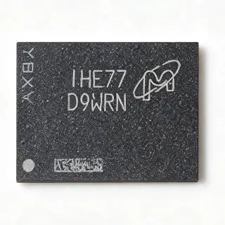
MT53B256M32D1DS-062 - 8Gb LPDDR4 SDRAM 3200MT/s | Micron
MPN: MT53B256M32D1DS-062 ✓ Active| Qty | Unit Price | Extended |
|---|---|---|
| 1 | $9.8 | $9.80 |
| 10 | $9.12 | $91.20 |
| 100 | $8.55 | $855.00 |
| 500 | $7.9 | $3,950.00 |
| 1,000 | $7.35 | $7,350.00 |
MT53B256M32D1DS-062 Overview
LPDDR4 (Low Power Double Data Rate 4) is a JEDEC-defined mobile DRAM standard optimized for high bandwidth and low power in battery-operated and thermally constrained systems. In the memory hierarchy, it sits as a main-memory DRAM component below cache SRAM and above storage NAND, serving as the working memory directly attached to application processors, SoCs, and FPGAs.
Key features of this device include the 8Gbit density in a single-die package, a wide 32-bit data bus, LPDDR4 core operation from a nominal 1.1V supply, and low-voltage signaling (VDDQ 1.1V class) that reduces I/O power compared with DDR3L. The -062 speed grade denotes a 625 ps clock cycle (1.6 GHz clock, 3200 MT/s data rate), enabling peak bus bandwidth of approximately 12.8 GB/s per 32-bit channel.
Architecturally, the device uses an 8n-prefetch banked DRAM core with burst lengths of 16 (BL16), on-die termination, and LPDDR4 power-down and self-refresh modes for aggressive idle-power management, making it suitable for sustained memory bandwidth workloads with duty-cycled power profiles.
Typical applications include mobile handset main memory, embedded vision and edge-AI SoC memory, automotive infotainment and ADAS platforms, networking appliances, and FPGA-based processing systems requiring high-bandwidth low-power DRAM.
A key design consideration is signal integrity on the CA and DQ buses: LPDDR4 routing requires length-matched fly-by or point-to-point topologies, controlled impedance, and accurate read/write training in the memory controller, so PCB stack-up and SoC memory-controller support must be confirmed early.
This page synthesizes distributor pricing, drop-in grade variants, and practical design notes not found in the manufacturer datasheet alone.
Drop-in alternatives for MT53B256M32D1DS-062 — same package, pin-to-pin compatible. Different-package parts requiring PCB rework are excluded.
Variants in this series
Same-series models that are drop-in compatible with MT53B256M32D1DS-062 (same form factor and footprint) — differing in Interface, Memory Type, Organization, Package.
Quick Comparison Tool — Select alternative parts for side-by-side comparison:
MT53B256M32D1DS-062 XT:C
✅ Drop-In📋 Reference alternative (not in catalog)
MT53B256M32D1DS-062 AIT:C
✅ Drop-In📋 Reference alternative (not in catalog)
MT53B256M32D1DS-062 AUT:C
✅ Drop-In📋 Reference alternative (not in catalog)
MT53B256M32D1DS-062 AAT:C
✅ Drop-In📋 Reference alternative (not in catalog)
MT53B256M32D1DT-062
✅ Drop-In ⚠️ Specs Unverified📋 Reference alternative (not in catalog)
MT53B256M32D1DS-062 Maximum Ratings & Electrical Characteristics
| Memory Type | Mobile LPDDR4 SDRAM |
| Memory Density | 8 Gbit |
| Organization | 256M x 32 |
| Clock Frequency | 1.6 GHz |
| Clock Cycle Time (tCK) | 625 ps (-062 speed grade) |
| Data Rate | 3200 MT/s per pin |
| Supply Voltage (VDD) | 1.1 V (typical, LPDDR4 class) |
| Package | 200-WFBGA (10 x 14.5 mm) |
| Mounting Type | Surface Mount |
| Interface | LPDDR4 (JEDEC mobile DRAM interface) |
| Burst Length | BL16 |
| Peak Bus Bandwidth | 12.8 GB/s (32-bit bus at 3200 MT/s) |
| RoHS Status | Compliant |
| Packaging | Tray (AAT:C) or Tape & Reel (TR suffix variants) |
MT53B256M32D1DS-062 200-wfbga (10 x 14.5 mm) Pin Configuration Guide
Pin configuration for MT53B256M32D1DS-062 (200-wfbga (10 x 14.5 mm) package). This digital IC includes GPIO, communication interfaces (UART, SPI, I2C), and power pins. Refer to the manufacturer datasheet for alternate pin functions and configuration options. Essential for embedded system design and PCB layout.

No detailed pinout data available for MT53B256M32D1DS-062.
Refer to the datasheet for full pin configuration.
Typical Applications
MT53B256M32D1DS-062 is suitable for 6 applications: Mobile and Tablet Main Memory, Edge-AI and Embedded Vision SoC Memory, Automotive Infotainment and ADAS, FPGA Processing and Prototyping Boards, Industrial Compute and Networking Appliances, Battery-Powered IoT and Portable Instruments.
Mobile and Tablet Main Memory
The MT53B256M32D1DS-062 is architected for exactly this market: an 8Gbit LPDDR4 die on a 32-bit bus running at 3200 MT/s provides the approximately 12.8 GB/s peak bandwidth modern application processors expect, while the 1.1V-class supply keeps memory power within smartphone thermal budgets. In a handset, the device attaches point-to-point to the SoC's LPDDR4 controller with length-matched CA/DQ routing; BL16 bursts and on-die termination minimize reflection-induced eye closure at 1.6 GHz. Power-down and self-refresh states let the OS gate memory current during idle periods, directly extending battery life. The 200-WFBGA 10x14.5 mm outline fits standard mobile PCB keep-outs.
Recommended
Edge-AI and Embedded Vision SoC Memory
Edge-AI accelerators and vision SoCs stream frame buffers and activation tensors to DRAM continuously, so bandwidth, not just capacity, sets performance. The MT53B256M32D1DS-062's 3200 MT/s data rate on a 32-bit bus supplies roughly 12.8 GB/s of peak bandwidth for real-time multi-camera image pipelines, while its 8Gbit capacity holds 1080p/4K frame buffers plus neural-network intermediates. The 1.1V-class LPDDR4 interface keeps total power low enough for fanless embedded enclosures. Designers should budget PCB layers for length-matched fly-by routing and verify the SoC memory controller's LPDDR4 training support at the -062 speed grade before tape-out.
Recommended
Automotive Infotainment and ADAS
Automotive cockpit SoCs and ADAS platforms need DRAM that survives wide ambient temperatures while sustaining graphics and sensor-fusion bandwidth. The MT53B256M32D1DS-062 AUT:C grade is Micron's automotive-positioned variant of this exact 8Gbit 256Mx32 die in the 200-WFBGA (10x14.5) package, allowing a single layout to be qualified across industrial and automotive programs. Its 3200 MT/s data rate supports multi-display infotainment rendering and radar/camera data buffering, and LPDDR4 self-refresh preserves system state during standby power modes. Confirm the exact AEC qualification class of the chosen suffix with Micron documentation during platform qualification.
Recommended
FPGA Processing and Prototyping Boards
High-end FPGAs and SoC-FPGAs with hard LPDDR4 memory controllers pair naturally with the MT53B256M32D1DS-062: the 256M x 32 organization matches single-channel LPDDR4 IP, and the 1.6 GHz clock (-062 grade) exercises the controller's full training capability. On an FPGA board, the 8Gbit device provides 1 GB of working memory for DSP pipelines, packet buffers, and RTL prototyping workloads. Because LPDDR4 requires per-device read/write training, designers should confirm the FPGA memory IP supports 3200 MT/s and validate PCB length matching; a successful bring-up then yields a reference for volume production layouts using the same footprint.
Recommended
Industrial Compute and Networking Appliances
Industrial gateways, network appliances, and edge servers require main memory with both bandwidth and low steady-state power. The MT53B256M32D1DS-062's 12.8 GB/s peak bandwidth handles packet buffering and protocol processing at multi-gigabit line rates, while LPDDR4 power-down modes cut idle draw versus DDR3/DDR4 alternatives - valuable in passively cooled enclosures. The AIT:C industrial grade of this same die supports extended ambient environments typical of factory floors and outdoor cabinets. Layout teams should follow the fly-by clock/CA routing rules in the Micron datasheet and reserve copper for the 1.1V rail, which carries substantial transient current during BL16 bursts.
Recommended
Battery-Powered IoT and Portable Instruments
Portable instruments and high-end IoT gateways gain from LPDDR4's bandwidth-per-watt advantage: the MT53B256M32D1DS-062 runs from a 1.1V-class supply and offers deep power-down and self-refresh modes that reduce memory standby current to the microamp-to-milliamp range between wake events. Its 1 GB capacity supports local data logging, protocol stacks, and on-device analytics without external storage traffic. Because the 200-WFBGA (10x14.5 mm) package requires controlled-impedance routing, it suits four-layer or higher PCBs typical of these products; designs should implement the datasheet power-up sequence and ZQ calibration resistor placement for reliable initialization across battery voltage sag.
Recommended
Recommended Products Summary
Engineering reference data for MT53B256M32D1DS-062 — comparison, design guidance, and compliance information.
Selection Guide
Comparison with Alternatives
| Parameter | This Product | MT53B256M32D1DS-062 XT:C | MT53B256M32D1DS-062 AIT:C | MT53B256M32D1DS-062 AUT:C | MT53B256M32D1DT-062 |
|---|---|---|---|---|---|
| Package | 200-WFBGA (10 x 14.5 mm) | 200-WFBGA (10 x 14.5 mm) - same | 200-WFBGA (10 x 14.5 mm) - same | 200-WFBGA (10 x 14.5 mm) - same | 200-WFBGA (10 x 14.5 mm) - same family |
| Brand | Micron Technology | Micron Technology | Micron Technology | Micron Technology | Micron Technology |
| Density | 8 Gbit | 8 Gbit | 8 Gbit | 8 Gbit | 8 Gbit |
| Organization | 256M x 32 | 256M x 32 | 256M x 32 | 256M x 32 | 256M x 32 |
| Clock Frequency | 1.6 GHz (-062 grade) | 1.6 GHz | 1.6 GHz | 1.6 GHz | 1.6 GHz |
| Qualification Grade | Standard (base -062 designation) | Extended grade | Industrial grade | Automotive-positioned grade | DT die revision |
| Memory Type | Mobile LPDDR4 SDRAM | Mobile LPDDR4 SDRAM | Mobile LPDDR4 SDRAM | Mobile LPDDR4 SDRAM | Mobile LPDDR4 SDRAM |
| Supply Voltage | 1.1 V class (LPDDR4) | 1.1 V class | 1.1 V class | 1.1 V class | 1.1 V class |
Key Differentiators
- Extended-temperature option without redesign (vs MT53B256M32D1DS-062 AAT:C)
- Automotive-positioned grade available (vs MT53B256M32D1DS-062 AUT:C)
- 32-bit single-die bandwidth advantage (vs MT53B128M32D1DS-062)
Design Notes
LPDDR4 at 3200 MT/s (1.6 GHz clock) leaves little timing margin: route the CA bus in fly-by topology and keep DQ/DQS nets length-matched within the tolerances specified in the Micron MT53B256M32D1 datasheet (typically on the order of a few mils per group - use the datasheet values, not rules of thumb). Control single-ended impedance near 40-50 ohm class per the JEDEC LPDDR4 signaling environment and reference DQ/CA nets to a solid VDDQ plane. Simulate eye diagrams on the DQS strobes before fabrication; at 625 ps tCK, even 20 ps of skew consumes meaningful margin in read/write training.
Provide tightly regulated 1.1V-class VDD and VDDQ rails with decoupling placed directly at the WFBGA ballouts per the datasheet decoupling network. During BL16 bursts the device draws large transient currents at 1.6 GHz, so pair bulk capacitance with multiple 0.1 uF/0.01 uF ceramics at each power ball. Implement the datasheet power-up sequence and CKE timing exactly; LPDDR4 devices can fail initialization or train incorrectly if VDD ramps too slowly or VDDQ precedes VDD out of spec. Route the 1.1V rail with wide copper and multiple vias to limit IR drop.
Do not mix suffix grades blindly: AAT, AIT, AUT, and XT variants of the MT53B256M32D1DS-062 differ in temperature qualification and packing, so a BOM swap between grades must be checked against the product's ambient range. Also confirm the memory controller supports the exact die revision (DS vs DT) address map; LPDDR4 mode-register programming and training algorithms are controller-side and must be revalidated when second-sourcing. Finally, avoid third-party sourcing for this part - mobile DRAM is a frequent target of remarked units; buy through authorized distributors to guarantee date-code traceability.
Compliance Information
RoHS compliance per distributor listings for the MT53B256M32D1DS-062 family. AEC-Q100 applicability depends on suffix grade (AUT:C is the automotive-positioned variant); verify exact qualification status with Micron documentation.