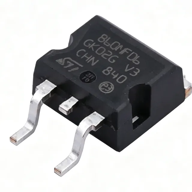
STB60NF06T4 - 60V, 60A N-Channel Power MOSFET | STMicroelectronics
MPN: STB60NF06T4 ✓ Active| Qty | Unit Price | Extended |
|---|---|---|
| 1 | $1.3636 | $1.36 |
| 10 | $0.9848 | $9.85 |
| 100 | $0.8712 | $87.12 |
| 500 | $0.8333 | $416.65 |
| 1,000 | $0.7955 | $795.50 |
STB60NF06T4 Overview
A Power MOSFET is a type of field-effect transistor optimized for power switching and amplification. It operates by controlling the flow of current between the drain and source terminals through an electric field applied at the gate. Power MOSFETs are widely used in power supplies, motor drives, and automotive applications due to their fast switching speed, high input impedance, and low conduction losses. They are a key component in the power management hierarchy, from discrete transistors to integrated power modules.
Key features of the STB60NF06T4 include a very low on-resistance of 14 mΩ, which minimizes conduction losses and improves efficiency in high-current paths. The device also offers a high avalanche ruggedness, with an avalanche energy rating of 300 mJ, making it suitable for applications with inductive loads. The gate charge is 60 nC, enabling fast switching and reduced switching losses. The device is RoHS compliant and halogen-free, meeting modern environmental standards.
The STB60NF06T4 utilizes STMicroelectronics' advanced PowerMESH™ technology, which provides a superior figure of merit (FOM) compared to conventional MOSFETs. This technology reduces the on-resistance and gate charge, resulting in lower power dissipation and improved thermal performance. The device also features a built-in Zener diode for ESD protection, enhancing its robustness in harsh environments.
Typical applications include DC-DC converters, motor control, power supplies, and automotive systems such as electric power steering and battery management. The low RDS(on) and high current capability make it ideal for synchronous rectification and load switching. In automotive applications, the device's ability to handle high surge currents and its wide operating temperature range (-55°C to 175°C) ensure reliable operation.
When designing with the STB60NF06T4, it is important to consider the thermal management. The D2PAK package has a thermal resistance of 62.5°C/W (junction-to-ambient) and 1.0°C/W (junction-to-case). For high-current applications, a heatsink or adequate PCB copper area is required to keep the junction temperature within safe limits. Additionally, proper gate drive voltage (typically 10V) is necessary to achieve the lowest on-resistance.
Drop-in alternatives for STB60NF06T4 — same package, pin-to-pin compatible. Different-package parts requiring PCB rework are excluded.
Variants in this series
Same-series models that are drop-in compatible with STB60NF06T4 (same form factor and footprint).
Quick Comparison Tool — Select alternative parts for side-by-side comparison:
IRF3205
✓ In Stock
$0.74 / Unit
View Datasheet →STB60NF06
📋 Reference alternative (not in catalog)
STB60NF06T4-Q1
📋 Reference alternative (not in catalog)
STP60NF06
📋 Reference alternative (not in catalog)
NTD60N06
📋 Reference alternative (not in catalog)
STB60NF06T4 Maximum Ratings & Electrical Characteristics
| Polarity | N-Channel |
| Drain-Source Voltage (VDS) | 60 V |
| Continuous Drain Current (ID) at 25°C | 60 A |
| Continuous Drain Current (ID) at 100°C | 42 A |
| Pulsed Drain Current (IDM) | 240 A |
| On-Resistance (RDS(on)) at VGS=10V | 14 mΩ (typ), 18 mΩ (max) |
| Gate-Source Voltage (VGS) | ±20 V |
| Gate Charge (Qg) | 60 nC (typ) |
| Input Capacitance (Ciss) | 2200 pF (typ) |
| Output Capacitance (Coss) | 350 pF (typ) |
| Reverse Transfer Capacitance (Crss) | 120 pF (typ) |
| Avalanche Energy (EAS) | 300 mJ |
| Operating Temperature Range | -55°C to +175°C |
| Package | D2PAK (TO-263) |
| Mounting Type | Surface Mount |
| RoHS Status | Compliant |
| Halogen Free | Yes |
STB60NF06T4 Pin Configuration
| Pin 1 | Gate — Gate terminal for controlling the MOSFET |
| Pin 2 | Drain — Drain terminal, connected to the tab |
| Pin 3 | Source — Source terminal |
Safe Operating Area (DC)
Typical Applications
STB60NF06T4 is suitable for 6 applications: DC-DC Converters, Motor Control, Power Supplies, Automotive Systems, Battery Management Systems, Load Switching.
DC-DC Converters
The STB60NF06T4 is used in DC-DC converters for its low on-resistance and high current capability. In a typical buck converter, the MOSFET acts as a synchronous rectifier, switching at high frequency to regulate output voltage. The low RDS(on) of 14 mΩ minimizes conduction losses, improving efficiency. The device's fast switching speed, enabled by a gate charge of 60 nC, reduces switching losses. The D2PAK package allows efficient heat dissipation, essential for high-power converters. Designers must ensure proper gate drive voltage (10V) and adequate PCB copper area for thermal management.
Recommended
Motor Control
In motor control applications, the STB60NF06T4 is used in H-bridge or three-phase inverter circuits to drive DC or brushless DC motors. The high current rating (60A) and low on-resistance ensure efficient power delivery to the motor. The device's avalanche ruggedness (300 mJ) is crucial for handling inductive kickback from motor windings. The wide operating temperature range (-55°C to 175°C) makes it suitable for industrial and automotive environments. For PWM control, the MOSFET's fast switching reduces losses, but designers must consider gate drive requirements and snubber circuits to minimize ringing.
Recommended
Power Supplies
The STB60NF06T4 is used in switch-mode power supplies (SMPS) for primary-side switching and synchronous rectification. Its low RDS(on) reduces conduction losses, improving overall efficiency. The device's high voltage rating (60V) is suitable for 12V and 24V systems. The D2PAK package allows for compact designs with adequate thermal performance. In flyback or forward converters, the MOSFET's avalanche capability handles voltage spikes from the transformer. Designers should ensure proper snubber circuits and gate drive to optimize performance.
Recommended
Automotive Systems
In automotive applications, the STB60NF06T4 is used in electric power steering, battery management, and load switching. The device's wide temperature range and high surge current capability make it reliable in harsh environments. The low on-resistance minimizes power dissipation, which is critical in battery-powered systems. The device is not AEC-Q100 qualified, but the STB60NF06T4-Q1 variant is available for automotive-grade requirements. Designers must consider the thermal environment under the hood and use appropriate heatsinking.
Recommended
Battery Management Systems
The STB60NF06T4 is used in battery management systems (BMS) for cell balancing and load switching. Its low on-resistance ensures minimal voltage drop across the MOSFET, preserving battery energy. The high current rating supports high-discharge applications. The device's avalanche ruggedness is important for handling inductive loads from relays or contactors. The D2PAK package allows for efficient heat dissipation in compact BMS designs. Designers should ensure proper gate drive and protection against overvoltage.
Recommended
Load Switching
The STB60NF06T4 is used for general-purpose load switching in industrial and consumer applications. Its low RDS(on) and high current capability make it ideal for switching high-power loads such as heaters, lamps, and solenoids. The device's fast switching speed allows for efficient PWM dimming or control. The D2PAK package provides good thermal performance for continuous operation. Designers should consider inrush current and provide adequate gate drive.
Recommended
Recommended Products Summary
Engineering reference data for STB60NF06T4 — comparison, design guidance, and compliance information.
Selection Guide
Comparison with Alternatives
| Parameter | This Product | STB60NF06 | STB60NF06T4-Q1 | STP60NF06 | IRF3205 | NTD60N06 |
|---|---|---|---|---|---|---|
| Package | D2PAK (TO-263) | D2PAK (TO-263) - same | D2PAK (TO-263) - same | TO-220 - different | TO-220 - different | DPAK (TO-252) - different |
| Brand | STMicroelectronics | STMicroelectronics | STMicroelectronics | STMicroelectronics | Infineon | onsemi |
| Drain-Source Voltage (VDS) | 60 V | 60 V | 60 V | 60 V | 55 V | 60 V |
| Continuous Drain Current (ID) at 25°C | 60 A | 60 A | 60 A | 60 A | 110 A | 60 A |
| On-Resistance (RDS(on)) | 14 mΩ (typ) | 14 mΩ (typ) | 14 mΩ (typ) | 14 mΩ (typ) | 8 mΩ (typ) | 14 mΩ (typ) |
| Gate Charge (Qg) | 60 nC (typ) | 60 nC (typ) | 60 nC (typ) | 60 nC (typ) | 146 nC (typ) | 60 nC (typ) |
| Avalanche Energy (EAS) | 300 mJ | 300 mJ | 300 mJ | 300 mJ | 250 mJ | 300 mJ |
| Operating Temperature Range | -55°C to +175°C | -55°C to +175°C | -55°C to +175°C | -55°C to +175°C | -55°C to +175°C | -55°C to +175°C |
Key Differentiators
- Low on-resistance of 14 mΩ (vs IRF3205)
- Automotive-grade variant available (vs STB60NF06)
- High avalanche energy rating of 300 mJ (vs IRF3205)
Design Notes
The STB60NF06T4 in D2PAK package has a junction-to-case thermal resistance of 1.0°C/W and junction-to-ambient of 62.5°C/W. For continuous operation at 60A, power dissipation is I^2*R = 60^2 * 0.014 = 50.4W. This would require a heatsink or large PCB copper area to keep junction temperature below 175°C. Use thermal vias and a copper pour of at least 1 square inch for adequate heat spreading.
Place the gate drive circuit close to the MOSFET to minimize parasitic inductance. Use a gate resistor (typically 10Ω) to dampen ringing. Ensure the source connection is low-inductance for high-current paths. For high-frequency switching, use a low-ESR ceramic capacitor (100nF) near the drain and source pins for decoupling.
Do not exceed the maximum gate-source voltage of ±20V. Use a Zener diode or TVS for gate protection if the gate drive can overshoot. Ensure the drain-source voltage does not exceed 60V, especially during inductive switching. Use a snubber circuit or avalanche-rated device to handle voltage spikes.
Compliance Information
RoHS compliant and halogen-free per STMicroelectronics datasheet. Not AEC-Q100 qualified; automotive-grade variant STB60NF06T4-Q1 is available.
