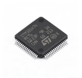
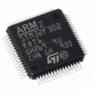
STM32F401RBT6 - ARM Cortex-M4 84MHz MCU | STMicroelectronics
MPN: STM32F401RBT6 ✓ Active| Qty | Unit Price | Extended |
|---|---|---|
| 1 | $6.5 | $6.50 |
| 10 | $5.85 | $58.50 |
| 100 | $5.2 | $520.00 |
| 500 | $4.68 | $2,340.00 |
| 1,000 | $4.16 | $4,160.00 |
STM32F401RBT6 Overview
What is a microcontroller (MCU)? A microcontroller is a compact integrated circuit designed to govern a specific operation in an embedded system. It integrates a processor core, memory (Flash and SRAM), and programmable input/output peripherals on a single chip. In the system hierarchy, an MCU is a type of embedded processor, which falls under the broader category of integrated circuits. The STM32F401RBT6 is a mid-range MCU in the STM32F4 family, positioned between the entry-level STM32F0 and the high-performance STM32F7 series, offering a balance of performance, power efficiency, and cost.
Key features of the STM32F401RBT6 include an ARM Cortex-M4 core with FPU, 84 MHz maximum clock speed, 128 KB Flash, 64 KB SRAM, and a rich set of peripherals: 3 USARTs, 4 SPIs, 3 I2Cs, 1 USB 2.0 OTG FS, 1 SDIO, 1 ADC (12-bit, 16 channels), and multiple timers. It operates from a 1.7V to 3.6V power supply and supports a temperature range of -40°C to +85°C. The device includes a 12-bit ADC with up to 16 channels, enabling precise analog signal acquisition. It also features a true random number generator (RNG) and a CRC calculation unit for data integrity.
Technically, the STM32F401RBT6 is built on a 90nm process technology, offering a good balance of performance and power consumption. The Cortex-M4 core with FPU accelerates mathematical computations, making it suitable for DSP and control applications. The device supports multiple low-power modes (Sleep, Stop, Standby) to optimize energy consumption in battery-powered designs. The LQFP64 package provides 50 GPIOs, with many pins multiplexed to support various peripheral functions, offering design flexibility.
Typical applications include industrial control systems, motor drives, consumer electronics, IoT devices, and medical monitoring equipment. Its combination of processing power, peripheral set, and low-power modes makes it ideal for applications requiring real-time control and connectivity. For example, in a smart home gateway, the STM32F401RBT6 can manage sensor data acquisition, run communication protocols (e.g., Zigbee, Bluetooth), and control actuators.
When designing with this MCU, ensure proper decoupling of the power supply pins with 100nF capacitors placed close to each VDD pin, and a 4.7uF bulk capacitor. The VDDA pin should be filtered with a ferrite bead and capacitor to reduce analog noise. Also, configure the clock source (HSE or HSI) appropriately and use the PLL to achieve the desired system clock. For low-power applications, utilize the Stop and Standby modes with wake-up sources like RTC or external interrupts.
Drop-in alternatives for STM32F401RBT6 — same package, pin-to-pin compatible. Different-package parts requiring PCB rework are excluded.
Variants in this series
Same-series models that are drop-in compatible with STM32F401RBT6 (same form factor and footprint) — differing in Timers, Flash Memory, SRAM, ADC, Core.
Quick Comparison Tool — Select alternative parts for side-by-side comparison:
STM32F401RCT6
✅ Drop-In ⚠️ 参数待验证✓ In Stock
$2.65 / Unit
View Datasheet →STM32F401RET6
✅ Drop-In ⚠️ 参数待验证✓ In Stock
$5.44 / Unit
View Datasheet →STM32F411RET6
✅ Drop-In ⚠️ 参数待验证✓ In Stock
$4.02 / Unit
View Datasheet →STM32F405RGT6
✅ Drop-In ⚠️ 参数待验证✓ In Stock
$6.75 / Unit
View Datasheet →ATSAMD51J19A
✅ Drop-In ⚠️ 参数待验证📋 Reference alternative (not in catalog)
LPC1768FBD100
✅ Drop-In ⚠️ 参数待验证📋 Reference alternative (not in catalog)
STM32F401RBT6 Maximum Ratings & Electrical Characteristics
| Core | ARM Cortex-M4 with FPU |
| Maximum Clock Speed | 84 MHz |
| Flash Memory | 128 KB |
| SRAM | 64 KB |
| Supply Voltage | 1.7 V to 3.6 V |
| Operating Temperature | -40C to +85C |
| Package | LQFP-64 (10x10 mm) |
| GPIO Pins | 50 |
| ADC | 12-bit, 16 channels |
| USART | 3 |
| SPI | 4 |
| I2C | 3 |
| USB | 1x USB 2.0 OTG FS |
| Timers | 8 (including advanced-control) |
| DMA | Yes, 8 channels |
| RTC | Yes |
| Low Power Modes | Sleep, Stop, Standby |
| RoHS | Compliant |
STM32F401RBT6 Pin Configuration
| Pin 1 | VBAT — Backup battery supply for RTC and backup registers |
| Pin 2 | PC13 — GPIO or RTC tamper/calendar |
| Pin 3 | PC14 — GPIO or OSC32_IN |
| Pin 4 | PC15 — GPIO or OSC32_OUT |
| Pin 5 | PF0 — GPIO or OSC_IN |
| Pin 6 | PF1 — GPIO or OSC_OUT |
| Pin 7 | NRST — Reset (active low) |
| Pin 8 | VSSA — Analog ground |
| Pin 9 | VDDA — Analog power supply |
| Pin 10 | PA0 — GPIO/ADC12_IN0/TIM2_CH1 |
| Pin 11 | PA1 — GPIO/ADC12_IN1/TIM2_CH2 |
| Pin 12 | PA2 — GPIO/ADC12_IN2/TIM2_CH3/USART2_TX |
| Pin 13 | PA3 — GPIO/ADC12_IN3/TIM2_CH4/USART2_RX |
| Pin 14 | VSS — Ground |
| Pin 15 | VDD — Power supply |
| Pin 16 | PA4 — GPIO/ADC12_IN4/SPI1_NSS |
| Pin 17 | PA5 — GPIO/ADC12_IN5/SPI1_SCK |
| Pin 18 | PA6 — GPIO/ADC12_IN6/SPI1_MISO |
| Pin 19 | PA7 — GPIO/ADC12_IN7/SPI1_MOSI |
| Pin 20 | PB0 — GPIO/ADC12_IN8/TIM3_CH3 |
| Pin 21 | PB1 — GPIO/ADC12_IN9/TIM3_CH4 |
| Pin 22 | PB2 — GPIO/BOOT1 |
| Pin 23 | PB10 — GPIO/I2C2_SCL/USART3_TX |
| Pin 24 | PB11 — GPIO/I2C2_SDA/USART3_RX |
| Pin 25 | VSS — Ground |
| Pin 26 | VDD — Power supply |
| Pin 27 | PB12 — GPIO/SPI2_NSS/I2C2_SMBA |
| Pin 28 | PB13 — GPIO/SPI2_SCK |
| Pin 29 | PB14 — GPIO/SPI2_MISO |
| Pin 30 | PB15 — GPIO/SPI2_MOSI |
| Pin 31 | PC6 — GPIO/TIM3_CH1/SDIO_D6 |
| Pin 32 | PC7 — GPIO/TIM3_CH2/SDIO_D7 |
| Pin 33 | PC8 — GPIO/TIM3_CH3/SDIO_D0 |
| Pin 34 | PC9 — GPIO/TIM3_CH4/SDIO_D1 |
| Pin 35 | PA8 — GPIO/USART1_CK/TIM1_CH1 |
| Pin 36 | PA9 — GPIO/USART1_TX/TIM1_CH2 |
| Pin 37 | PA10 — GPIO/USART1_RX/TIM1_CH3 |
| Pin 38 | PA11 — GPIO/USART1_CTS/USB_DM |
| Pin 39 | PA12 — GPIO/USART1_RTS/USB_DP |
| Pin 40 | PA13 — GPIO/SWDIO |
| Pin 41 | VSS — Ground |
| Pin 42 | VDD — Power supply |
| Pin 43 | PA14 — GPIO/SWCLK |
| Pin 44 | PA15 — GPIO/JTDI/TIM2_CH1 |
| Pin 45 | PB3 — GPIO/JTDO/TRACESWO |
| Pin 46 | PB4 — GPIO/NJTRST |
| Pin 47 | PB5 — GPIO/I2C1_SMBA |
| Pin 48 | PB6 — GPIO/I2C1_SCL/TIM4_CH1 |
| Pin 49 | PB7 — GPIO/I2C1_SDA/TIM4_CH2 |
| Pin 50 | BOOT0 — Boot mode selection |
| Pin 51 | PB8 — GPIO/I2C1_SCL/TIM4_CH3 |
| Pin 52 | PB9 — GPIO/I2C1_SDA/TIM4_CH4 |
| Pin 53 | VSS — Ground |
| Pin 54 | VDD — Power supply |
| Pin 55 | PC0 — GPIO/ADC12_IN10 |
| Pin 56 | PC1 — GPIO/ADC12_IN11 |
| Pin 57 | PC2 — GPIO/ADC12_IN12 |
| Pin 58 | PC3 — GPIO/ADC12_IN13 |
| Pin 59 | PC4 — GPIO/ADC12_IN14 |
| Pin 60 | PC5 — GPIO/ADC12_IN15 |
| Pin 61 | PB12 — GPIO/SPI2_NSS/I2C2_SMBA |
| Pin 62 | PB13 — GPIO/SPI2_SCK |
| Pin 63 | PB14 — GPIO/SPI2_MISO |
| Pin 64 | PB15 — GPIO/SPI2_MOSI |
Typical Applications
STM32F401RBT6 is suitable for 6 applications: Industrial Control, IoT Devices, Consumer Electronics, Medical Monitoring, Automotive Aftermarket, Education and Prototyping.
Industrial Control
The STM32F401RBT6 is ideal for industrial control systems such as PLCs, motor drives, and robotic controllers. Its 84 MHz Cortex-M4 core with FPU accelerates real-time control algorithms, while the advanced timers generate precise PWM signals. The 12-bit ADC with 16 channels enables accurate sensor feedback. In a typical motor drive, the MCU reads current sensors via ADC, computes FOC, and outputs PWM to the inverter. The wide supply voltage range (1.7V-3.6V) and -40°C to +85°C operation ensure reliability in harsh environments. Compared to lower-end MCUs, the FPU reduces computation time for complex control loops, improving system responsiveness.
Recommended
IoT Devices
For IoT applications, the STM32F401RBT6 provides a balance of processing power and low-power modes. It supports Sleep, Stop, and Standby modes, with wake-up from RTC or external interrupts, enabling battery-powered devices to achieve long battery life. The USB 2.0 OTG FS interface allows direct connection to smartphones or PCs for data transfer and firmware updates. The 128 KB Flash is sufficient for communication stacks like MQTT, CoAP, or Bluetooth LE (via external module). In a smart home sensor node, the MCU periodically wakes from Stop mode, reads sensors, transmits data via a sub-GHz radio, and returns to sleep, consuming only microamps in standby. The rich peripheral set (USART, SPI, I2C) simplifies interfacing with various sensors and wireless modules.
Recommended
Consumer Electronics
The STM32F401RBT6 is widely used in consumer electronics such as smart appliances, wearables, and gaming peripherals. Its compact LQFP64 package and low power consumption make it suitable for space-constrained designs. The USB OTG interface enables direct connection to PCs for charging and data sync. The Cortex-M4 FPU accelerates audio processing, making it possible to implement simple audio effects or voice recognition. In a smart speaker, the MCU can handle audio codec control, button inputs, and LED indicators, while offloading heavy processing to a dedicated DSP. The 84 MHz clock ensures smooth user interface responsiveness. The device's wide operating voltage range allows it to be powered from a single Li-ion battery (3.3V) or USB 5V with an LDO.
Recommended
Medical Monitoring
In medical monitoring devices like patient vital sign monitors and portable ECG devices, the STM32F401RBT6 offers the processing power and analog capabilities needed for signal acquisition and processing. The 12-bit ADC with 16 channels can sample multiple biosignals simultaneously, while the Cortex-M4 FPU accelerates digital filtering and feature extraction. The low-power modes are crucial for battery-operated wearable monitors. For example, in a heart rate monitor, the MCU reads PPG sensor data via ADC, applies a bandpass filter, and computes heart rate using a peak detection algorithm. The USB interface allows data logging to a PC. The device's reliability and long-term availability make it suitable for medical applications, though certification (e.g., IEC 60601) is required for end products.
Recommended
Automotive Aftermarket
The STM32F401RBT6 is used in automotive aftermarket products such as car diagnostic tools, GPS trackers, and infotainment systems. Its robust design and wide temperature range (-40°C to +85°C) make it suitable for under-hood or cabin environments. The CAN interface (though not listed in the basic specs, it is available in some variants) can be added via external transceiver for OBD-II diagnostics. The USB OTG interface enables connection to smartphones for data display. In a GPS tracker, the MCU reads GPS data via UART, processes location information, and transmits it via a cellular module. The low-power modes help reduce battery drain when the vehicle is off. The device's rich peripheral set simplifies interfacing with GPS modules, cellular modems, and display controllers.
Recommended
Education and Prototyping
The STM32F401RBT6 is popular in education and rapid prototyping due to its low cost, availability, and extensive community support. It is used in development boards like the STM32F401RE Nucleo and Black Pill, which are widely used in university courses and maker projects. The STM32CubeIDE and HAL libraries simplify development, allowing students to focus on application logic. The device's performance is sufficient for learning RTOS, embedded C, and digital signal processing. In a robotics project, the MCU can control motors, read sensors, and implement PID control. The LQFP64 package is easy to solder with a hot-air station, and the 0.5mm pitch is manageable for hobbyists. The availability of many tutorials and examples accelerates the learning curve.
Recommended
Recommended Products Summary
Engineering reference data for STM32F401RBT6 — comparison, design guidance, and compliance information.
Selection Guide
Comparison with Alternatives
| Parameter | This Product | STM32F401RCT6 | STM32F401RET6 | STM32F411RET6 | STM32F405RGT6 | ATSAMD51J19A | LPC1768FBD100 |
|---|---|---|---|---|---|---|---|
| Package | LQFP-64 | LQFP-64 | LQFP-64 | LQFP-64 | LQFP-64 | LQFP-64 | LQFP-64 |
| Brand | STMicroelectronics | STMicroelectronics | STMicroelectronics | STMicroelectronics | STMicroelectronics | Microchip Technology | NXP Semiconductors |
| Core | ARM Cortex-M4 with FPU | ARM Cortex-M4 with FPU | ARM Cortex-M4 with FPU | ARM Cortex-M4 with FPU | ARM Cortex-M4 with FPU | ARM Cortex-M4F | ARM Cortex-M3 |
| Maximum Clock Speed | 84 MHz | 84 MHz | 84 MHz | 100 MHz | 168 MHz | 120 MHz | 100 MHz |
| Flash Memory | 128 KB | 256 KB | 512 KB | 512 KB | 1 MB | 512 KB | 512 KB |
| SRAM | 64 KB | 64 KB | 64 KB | 128 KB | 192 KB | 192 KB | 64 KB |
| ADC | 12-bit, 16 channels | 12-bit, 16 channels | 12-bit, 16 channels | 12-bit, 16 channels | 12-bit, 16 channels | 12-bit, 20 channels | 12-bit, 8 channels |
| USB | 1x USB 2.0 OTG FS | 1x USB 2.0 OTG FS | 1x USB 2.0 OTG FS | 1x USB 2.0 OTG FS | 1x USB 2.0 OTG FS | 1x USB 2.0 | 1x USB 2.0 FS/HS |
Key Differentiators
- Higher clock speed than STM32F401RCT6 (vs STM32F401RCT6)
- Lower power consumption than STM32F411RET6 (vs STM32F411RET6)
- Better ecosystem and software support than ATSAMD51J19A (vs ATSAMD51J19A)
Design Notes
Decouple each VDD pin with a 100nF ceramic capacitor placed as close as possible to the pin, and add a 4.7uF bulk capacitor. The VDDA pin should be connected to VDD through a ferrite bead and a 1uF capacitor to filter analog noise. Ensure VSSA is connected to ground with a low-impedance path. For battery-powered designs, use the VBAT pin for RTC backup and connect a 3V coin cell.
For the LQFP64 package, use a 4-layer PCB with a solid ground plane. Place the crystal (HSE) and load capacitors close to the OSC_IN/OSC_OUT pins, with a ground guard ring to reduce noise. Keep high-speed signals (e.g., SPI, USB) away from the crystal and analog pins. Use via stitching around the ground plane to minimize EMI.
Ensure the BOOT0 pin is properly configured: tie to GND for normal boot from Flash, or to VDD for boot from system memory. Do not leave NRST floating; connect a 100nF capacitor to GND. When using the ADC, set the sampling time appropriately for the source impedance to avoid inaccurate readings. Also, configure the PLL correctly to avoid exceeding the maximum clock speed of 84 MHz.
Compliance Information
RoHS compliant per STMicroelectronics product page. Not AEC-Q100 qualified; for automotive, consider STM32F401RBT6Q or other automotive-grade variants.