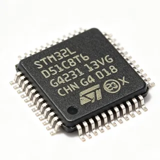
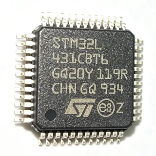
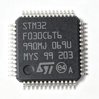
STM8AF5268TCY - 8-bit Automotive MCU, 32KB Flash, LQFP48 | STMicroelectronics
MPN: STM8AF5268TCY ✓ Active| Qty | Unit Price | Extended |
|---|---|---|
| 1 | $5.65 | $5.65 |
| 10 | $5.2 | $52.00 |
| 100 | $4.75 | $475.00 |
| 500 | $4.3 | $2,150.00 |
| 1,000 | $3.9 | $3,900.00 |
STM8AF5268TCY Overview
An 8-bit microcontroller (MCU) is a compact integrated circuit that executes instructions on 8-bit data words, typically used for control-oriented tasks in embedded systems. The STM8A core is an enhanced 8-bit architecture with a three-stage pipeline, offering high code density and efficient execution for cost-sensitive automotive modules. As a member of the STM8AF series, this MCU sits within the broader hierarchy of microcontrollers, which are themselves a subset of integrated circuits used in electronic control units (ECUs) across the automotive industry.
Key features include a rich set of peripherals: two UARTs, two SPI interfaces, two I2C interfaces, a 10-bit ADC with up to 16 channels, multiple 16-bit timers, and a CAN 2.0B controller. The device supports a supply voltage range of 3.0V to 5.5V, making it compatible with both 3.3V and 5V systems. It also includes an internal 16 MHz RC oscillator and a low-power RTC, reducing external component count. The automotive qualification (AEC-Q100 Grade 1) ensures operation from -40°C to +150°C ambient temperature, suitable for under-hood environments.
The STM8AF5268TCY is built on a robust 130nm embedded Flash process, providing high reliability and endurance (up to 100k write/erase cycles). The CAN controller supports both 2.0A and 2.0B protocols, enabling seamless integration into vehicle networks. The device also features a 10-bit ADC with programmable sampling time, which is essential for accurate sensor readings in engine management and battery monitoring.
Typical applications include body control modules (BCM), door and window control, seat control, HVAC (heating, ventilation, and air conditioning) systems, and lighting control. Its CAN interface makes it ideal for distributed automotive networks, while the low-power modes (Halt, Active-Halt, Wait) help meet stringent quiescent current requirements in battery-backed systems.
When designing with this MCU, ensure proper decoupling of the VDD and VDDA pins with 100nF capacitors placed close to the device. The internal RC oscillator is factory-calibrated to ±1% accuracy, but for applications requiring higher precision, an external crystal can be connected to the OSC_IN/OSC_OUT pins. The device supports in-application programming (IAP) via the bootloader, simplifying firmware updates in the field.
Drop-in alternatives for STM8AF5268TCY — same package, pin-to-pin compatible. Different-package parts requiring PCB rework are excluded.
Variants in this series
Same-series models that are drop-in compatible with STM8AF5268TCY (same form factor and footprint) — differing in Number of I/O Pins, Package, Supply Voltage Range, Timers.
Quick Comparison Tool — Select alternative parts for side-by-side comparison:
STM8AF5288TC
✅ Drop-In📋 Reference alternative (not in catalog)
STM8S207C6T6
✅ Drop-In📋 Reference alternative (not in catalog)
STM8AF5268TCX
✅ Drop-In ⚠️ Specs Unverified📋 Reference alternative (not in catalog)
STM8AF5268TCY Maximum Ratings & Electrical Characteristics
| Core | STM8A |
| Architecture | 8-bit CISC |
| Maximum Clock Frequency | 24 MHz |
| Flash Program Memory | 32 KB (32K x 8) |
| RAM Size | 2 KB |
| EEPROM Size | 1 KB |
| Supply Voltage Range | 3.0 V to 5.5 V |
| Number of I/O Pins | 38 |
| ADC Resolution | 10-bit |
| ADC Channels | 16 |
| CAN Interface | Yes (2.0A/2.0B) |
| UART Interfaces | 2 |
| SPI Interfaces | 2 |
| I2C Interfaces | 2 |
| Timers | Multiple 16-bit |
| Package | LQFP-48 (7x7 mm) |
| Mounting Type | Surface Mount |
| Operating Temperature Range | -40°C to +150°C |
| Automotive Qualification | AEC-Q100 Grade 1 |
| RoHS Status | Compliant |
STM8AF5268TCY Pin Configuration
| Pin 1 | VSS — Ground |
| Pin 2 | VDD — Power supply (3.0V-5.5V) |
| Pin 3 | PA0 — General purpose I/O / ADC input |
| Pin 4 | PA1 — General purpose I/O / ADC input |
| Pin 5 | PA2 — General purpose I/O / ADC input |
| Pin 6 | PA3 — General purpose I/O / ADC input |
| Pin 7 | VSSA — Analog ground |
| Pin 8 | VDDA — Analog power supply |
| Pin 9 | PB0 — General purpose I/O / SPI |
| Pin 10 | PB1 — General purpose I/O / SPI |
| Pin 11 | PB2 — General purpose I/O / SPI |
| Pin 12 | PB3 — General purpose I/O / SPI |
| Pin 13 | PB4 — General purpose I/O / I2C |
| Pin 14 | PB5 — General purpose I/O / I2C |
| Pin 15 | PB6 — General purpose I/O / UART |
| Pin 16 | PB7 — General purpose I/O / UART |
| Pin 17 | PC0 — General purpose I/O / ADC input |
| Pin 18 | PC1 — General purpose I/O / ADC input |
| Pin 19 | PC2 — General purpose I/O / ADC input |
| Pin 20 | PC3 — General purpose I/O / ADC input |
| Pin 21 | PC4 — General purpose I/O / ADC input |
| Pin 22 | PC5 — General purpose I/O / ADC input |
| Pin 23 | PC6 — General purpose I/O / ADC input |
| Pin 24 | PC7 — General purpose I/O / ADC input |
| Pin 25 | PD0 — General purpose I/O / CAN RX |
| Pin 26 | PD1 — General purpose I/O / CAN TX |
| Pin 27 | PD2 — General purpose I/O / UART |
| Pin 28 | PD3 — General purpose I/O / UART |
| Pin 29 | PD4 — General purpose I/O / SPI |
| Pin 30 | PD5 — General purpose I/O / SPI |
| Pin 31 | PD6 — General purpose I/O / I2C |
| Pin 32 | PD7 — General purpose I/O / I2C |
| Pin 33 | PE0 — General purpose I/O / Timer |
| Pin 34 | PE1 — General purpose I/O / Timer |
| Pin 35 | PE2 — General purpose I/O / Timer |
| Pin 36 | PE3 — General purpose I/O / Timer |
| Pin 37 | PE4 — General purpose I/O / Timer |
| Pin 38 | PE5 — General purpose I/O / Timer |
| Pin 39 | OSC_IN — External oscillator input |
| Pin 40 | OSC_OUT — External oscillator output |
| Pin 41 | NRST — Reset (active low) |
| Pin 42 | VSS — Ground |
| Pin 43 | VDD — Power supply (3.0V-5.5V) |
| Pin 44 | PF0 — General purpose I/O / ADC input |
| Pin 45 | PF1 — General purpose I/O / ADC input |
| Pin 46 | PF2 — General purpose I/O / ADC input |
| Pin 47 | PF3 — General purpose I/O / ADC input |
| Pin 48 | PF4 — General purpose I/O / ADC input |
Typical Applications
STM8AF5268TCY is suitable for 6 applications: Body Control Module (BCM), Engine Management System, HVAC Control System, Lighting Control Module, Seat Control Module, Battery Management System (BMS).
Body Control Module (BCM)
The STM8AF5268TCY is ideal for body control modules due to its CAN 2.0B interface, 24 MHz core, and AEC-Q100 Grade 1 qualification. It manages lighting, door locks, and window controls, with the 10-bit ADC reading sensor inputs and the CAN bus communicating with other ECUs. The wide 3.0V-5.5V supply range accommodates automotive battery voltage variations, while low-power modes reduce quiescent current when the vehicle is off. Its 32 KB Flash is sufficient for BCM firmware, and the 48-pin LQFP package fits compact module designs.
Recommended
Engine Management System
In engine management, the STM8AF5268TCY's 10-bit ADC with 16 channels reads sensors for temperature, pressure, and position. The 24 MHz core processes control loops in real-time, while the CAN interface connects to the vehicle network. The -40°C to +150°C operating range ensures reliability under hood, and the 100k write/erase cycle Flash endurance supports frequent calibration updates. The 2 KB RAM handles real-time data, and the 1 KB EEPROM stores non-volatile parameters. The 48-pin LQFP package fits on compact ECU boards.
Recommended
HVAC Control System
The STM8AF5268TCY controls HVAC systems by reading temperature sensors via its 10-bit ADC and driving actuators through PWM timers. The CAN interface allows integration with the vehicle's climate control network. Its low-power modes are crucial for maintaining battery life when the engine is off, and the wide supply voltage range handles system fluctuations. The 32 KB Flash stores control algorithms, and the 48-pin LQFP package fits within the HVAC control panel. AEC-Q100 Grade 1 ensures operation in extreme cabin temperatures.
Recommended
Lighting Control Module
The STM8AF5268TCY manages automotive lighting systems, including headlights, taillights, and interior lighting. Its 16-bit timers generate PWM signals for dimming, and the CAN interface receives commands from the BCM. The 10-bit ADC monitors current for fault detection, and the 3.0V-5.5V supply range supports various LED driver topologies. The AEC-Q100 Grade 1 qualification ensures reliable operation in harsh environments, and the 48-pin LQFP package fits within the lighting control unit. Low-power modes reduce drain when lights are off.
Recommended
Seat Control Module
The STM8AF5268TCY controls seat motors and memory functions. Its 16-bit timers generate PWM for motor speed control, and the 10-bit ADC reads position sensors for memory recall. The CAN interface communicates with the BCM and other modules. The 32 KB Flash stores seat position algorithms, and the 2 KB RAM handles real-time adjustments. The -40°C to +150°C range ensures operation in extreme climates, and the 48-pin LQFP package fits within the seat control unit. Low-power modes preserve battery when the seat is idle.
Recommended
Battery Management System (BMS)
The STM8AF5268TCY monitors battery voltage and current in automotive BMS applications. Its 10-bit ADC with 16 channels reads cell voltages and temperature sensors, while the CAN interface reports status to the vehicle network. The 1 KB EEPROM stores calibration data, and the 24 MHz core processes monitoring algorithms. The wide supply voltage range accommodates battery voltage variations, and the AEC-Q100 Grade 1 qualification ensures reliability. The 48-pin LQFP package fits within the BMS module, and low-power modes reduce drain when the vehicle is off.
Recommended
Recommended Products Summary
Engineering reference data for STM8AF5268TCY — comparison, design guidance, and compliance information.
Selection Guide
Comparison with Alternatives
| Parameter | This Product | STM8AF5288TC | STM8AF5268TAY | STM8S207C6T6 |
|---|---|---|---|---|
| Package | LQFP-48 | LQFP-48 (same) | LQFP-64 (different) | LQFP-48 (same) |
| Brand | STMicroelectronics | STMicroelectronics | STMicroelectronics | STMicroelectronics |
| Flash Memory | 32 KB | 64 KB | 32 KB | 128 KB |
| RAM Size | 2 KB | 6 KB | 2 KB | 6 KB |
| CAN Interface | Yes (2.0A/2.0B) | Yes (2.0A/2.0B) | Yes (2.0A/2.0B) | No |
| Automotive Qualification | AEC-Q100 Grade 1 | AEC-Q100 Grade 1 | AEC-Q100 Grade 1 | No |
| Operating Temperature | -40°C to +150°C | -40°C to +150°C | -40°C to +150°C | -40°C to +85°C |
| Number of I/O Pins | 38 | 38 | 52 | 38 |
Key Differentiators
- Automotive-grade CAN MCU with AEC-Q100 Grade 1 (vs STM8S207C6T6)
- True data EEPROM with 100k write/erase cycles (vs STM8AF5288TC)
- 48-pin LQFP package with 38 I/O pins (vs STM8AF5268TAY)
Design Notes
Decouple the VDD and VDDA pins with 100nF ceramic capacitors placed as close to the pins as possible. Additionally, place a 10uF bulk capacitor on the main VDD rail to handle transient currents. The VDDA pin should have a separate 100nF capacitor to isolate analog noise from digital switching.
For the LQFP-48 package, ensure proper solder paste stencil design with a 0.5mm pitch. Use a 4-layer PCB with a solid ground plane beneath the MCU to reduce EMI and improve thermal performance. Route the CAN bus lines with 120-ohm termination resistors at both ends of the bus.
Do not leave unused I/O pins floating; configure them as outputs or enable internal pull-ups. The NRST pin requires a 100nF capacitor to ground for reliable reset. When using the internal RC oscillator, note that it is calibrated to ±1% accuracy, which may not be sufficient for CAN communication - use an external crystal for CAN applications.
Compliance Information
AEC-Q100 Grade 1 qualified per STMicroelectronics. RoHS compliant. Conflict minerals policy follows STMicroelectronics corporate policy.