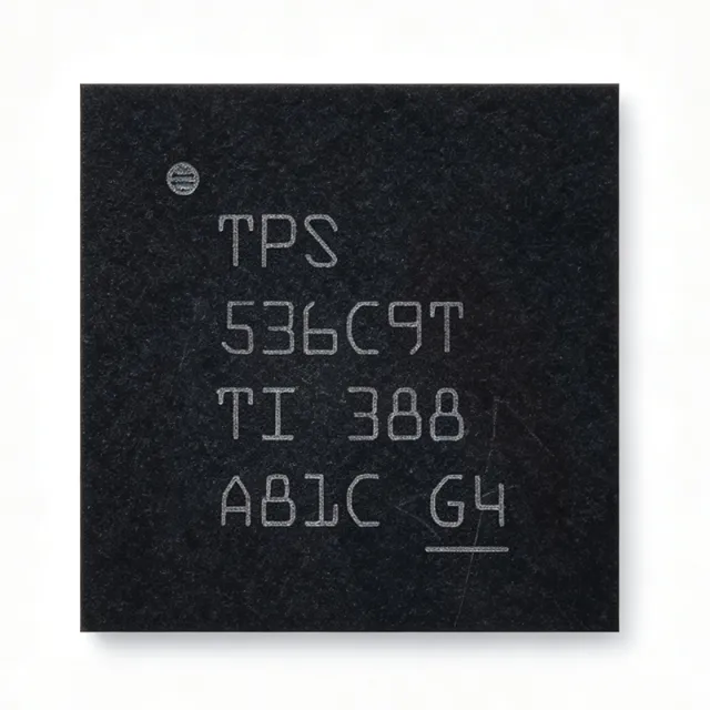
TPS536C9TRSLR - 12-Phase TLVR Buck Controller, 765A | TI
MPN: TPS536C9TRSLR ✓ Active| Qty | Unit Price | Extended |
|---|---|---|
| 1 | $0 | $0.00 |
| 10 | $0 | $0.00 |
| 100 | $0 | $0.00 |
| 500 | $0 | $0.00 |
| 1,000 | $0 | $0.00 |
TPS536C9TRSLR Overview
A multiphase buck controller is a power-management IC that orchestrates multiple power stages in parallel to deliver high current at low voltage, dividing current among phases for reduced ripple, better thermal distribution, and fast transient response. The TPS536C9T sits within the hierarchy of switching regulators as a controller-class device, pairing with external TI NexFET smart power stages to form a complete voltage regulator solution (VR) for processors.
Key features include native trans-inductor voltage regulator (TLVR) topology support with LC open and short protection, VR14 SVID interface compliance, and a PMBus interface for telemetry and configuration. Built-in non-volatile memory (NVM) stores configuration, and the D-CAP+ architecture provides fast transient response, low output capacitance, and accurate dynamic current sharing across phases.
The controller is fully compatible with TI NexFET smart power stages, allowing flexible N+M phase allocation (N+M <= 12, M <= 6) between the two channels. This scalability suits both compact dual-rail designs and high-current single-rail configurations used by modern server CPUs and GPUs.
Typical applications include server CPU core power (VR14 SVID rails), ASIC and FPGA point-of-load power, AI accelerator power delivery, and networking line-card processors requiring sub-1V, multi-hundred-amp rails with PMBus manageability.
Design tip: TI recommends keeping at least 800 mil distance between controller and power stages, sharing a common ground plane, and using the PMBus/NVM configuration flow during bring-up to tune loop response before production.
This page synthesizes verified datasheet parameters, drop-in alternatives, and practical design guidance not found on the manufacturer product page.
Drop-in alternatives for TPS536C9TRSLR — same package, pin-to-pin compatible. Different-package parts requiring PCB rework are excluded.
Variants in this series
Same-series models that are drop-in compatible with TPS536C9TRSLR (same form factor and footprint) — differing in Non-Volatile Memory, Package, Topology, Control Interface, Number of Channels.
Quick Comparison Tool — Select alternative parts for side-by-side comparison:
TPS536C9RSLR
✅ Drop-In✓ In Stock
$14.3182 / Unit
View Datasheet →TPS536C9T
✅ Drop-In✓ In Stock
$5.8 / Unit
View Datasheet →TPS536C9TRSLR Maximum Ratings & Electrical Characteristics
| Topology | Step-down multiphase buck controller (D-CAP+) |
| Number of Channels | 2 (N + M <= 12 phases, M <= 6) |
| Total Output Current | Up to 765 A (with 12 phases of power stages) |
| Input Voltage Range | 4.5 V to 17 V |
| Output Voltage Range | 0.25 V to 5.5 V |
| Control Interface | VR14 SVID and PMBus |
| TLVR Support | Native trans-inductor voltage regulator topology with LC open and short protection |
| Non-Volatile Memory | Built-in NVM for configuration |
| Power Stage Compatibility | TI NexFET smart power stages |
| Operating Temperature | -40C to +125C |
| Package | 48-pin VQFN (RSL) with exposed pad |
| Mounting Type | Surface Mount |
| Output Type | Positive, adjustable |
| Architecture | D-CAP+ (fast transient, dynamic current sharing) |
| Marking | TPS536C9T |
TPS536C9TRSLR 48-pin vqfn (rsl) with exposed pad Pin Configuration Guide
Pin configuration for TPS536C9TRSLR (48-pin vqfn (rsl) with exposed pad package). This power device features gate, drain, and source terminals. For non-polarized packages, refer to the manufacturer datasheet for exact pin 1 orientation and footprint details. Common applications include power supply design, motor driving, and load switching.

No detailed pinout data available for TPS536C9TRSLR.
Refer to the datasheet for full pin configuration.
Typical Applications
TPS536C9TRSLR is suitable for 6 applications: Server CPU Core Power (VR14), AI Accelerator Power Delivery, ASIC and FPGA Point-of-Load, Networking and Telecom Line Cards, Storage and Server Backplane Power, High-Density Multiphase Proof-of-Concept.
Server CPU Core Power (VR14)
The TPS536C9TRSLR is purpose-built for VR14 SVID-compliant CPU core rails in 1U/2U servers and motherboards. Its VR14 SVID interface lets the CPU command output voltage, offset, and active phase count in real time, while PMBus provides platform-level telemetry for current, voltage, and temperature. With N + M <= 12 phase capability and TI NexFET smart power stages, the controller sustains multi-hundred-amp core currents at sub-1V with tight dynamic regulation. D-CAP+ control keeps the loop fast enough for microsecond-class load steps, and NVM stores per-platform settings without external memory.
Recommended
AI Accelerator Power Delivery
AI accelerators present extreme transient loads - hundreds of amps stepping in microseconds - which the TPS536C9TRSLR addresses through native TLVR support and D-CAP+ control. The TLVR topology with LC open and short protection lets designers use coupled-inductor arrays to slash output capacitance while meeting tight transient budgets on sub-1V rails. Driving up to 12 phases of TI smart power stages, the controller scales to 765A-class solutions. PMBus telemetry supports fleet-level health monitoring of accelerator cards in data-center fleets, and runtime phase shedding maintains light-load efficiency during idle inference periods.
Recommended
ASIC and FPGA Point-of-Load
High-end ASICs and FPGAs need multiple precisely sequenced low-voltage rails, and the TPS536C9TRSLR covers this with two independently configurable channels and a 0.25V to 5.5V output range. The PMBus interface supports sequencing, margining, and fault management, while NVM retains configuration across power cycles without external EEPROM. D-CAP+ dynamic current sharing keeps rail accuracy high even during simultaneous channel load events, and the flexible N+M phase allocation (M <= 6) lets one controller serve both a large core rail and a smaller auxiliary rail, consolidating BOM and layout area on dense boards.
Recommended
Networking and Telecom Line Cards
Line-card processors and switch ASICs in networking equipment demand sub-1V, tens-to-hundreds-of-amp rails operating reliably from -40C to +85C ambient, which the TPS536C9TRSLR's -40C to +125C rating comfortably covers. PMBus manageability enables remote monitoring and fault logging required by carrier-grade platforms, and SVID-free operation is possible when no CPU is present by configuring Reset# with a pull-up and handling unused pins as TI's E2E forum guidance describes. TLVR support benefits the aggressive transient requirements of traffic-dependent ASIC load bursts in high-port-count switches.
Recommended
Storage and Server Backplane Power
Storage controllers and backplane-attached compute benefit from the TPS536C9TRSLR's dual-channel architecture: one channel powers a high-current SoC rail while the second serves a memory or ASIC rail from a single controller. The 4.5V to 17V input range accepts intermediate-bus voltages commonly found behind backplane DC-DC stages, and the 0.25V to 5.5V output range covers both modern sub-1V cores and legacy 5.5V logic. PMBus telemetry simplifies chassis-level manageability, while TLVR-equipped designs cut output capacitor count, valuable in space-constrained drive electronics.
Recommended
High-Density Multiphase Proof-of-Concept
For system bring-up and reference-design evaluation, the TPS536C9TRSLR's NVM plus PMBus configuration flow lets engineers tune loop response, phase allocation, and protection thresholds without hardware respins. TI's E2E layout guidance - at least 800 mil spacing between controller and power stages, common ground plane, and careful PWMx routing - applies directly to evaluation boards. The flexible N+M <= 12 phase allocation enables quick comparison of 8+4 versus 10+2 rail strategies on the same PCB, making the controller an efficient platform for characterizing NexFET power-stage pairings.
Recommended
Recommended Products Summary
Engineering reference data for TPS536C9TRSLR — comparison, design guidance, and compliance information.
Selection Guide
Comparison with Alternatives
| Parameter | This Product | TPS536C9RSLR | TPS536C9T |
|---|---|---|---|
| Package | 48-VQFN (RSL) exposed pad | 48-VQFN (RSL) - same | 48-VQFN (RSL) - same |
| Brand | Texas Instruments | Texas Instruments | Texas Instruments |
| Input Voltage Range | 4.5 V to 17 V | 4.5 V to 17 V | 4.5 V to 17 V |
| Output Voltage Range | 0.25 V to 5.5 V | 0.25 V to 5.5 V | 0.25 V to 5.5 V |
| Phase Configuration | N + M <= 12, M <= 6, dual channel | N + M <= 12, M <= 6, dual channel | N + M <= 12, M <= 6, dual channel |
| Interfaces | VR14 SVID + PMBus | VR14 SVID + PMBus | VR14 SVID + PMBus |
| Operating Temperature | -40C to +125C | -40C to +125C | -40C to +125C |
Key Differentiators
- Native TLVR topology support (vs TPS536C9RSLR)
- 12-phase dual-channel scalability (vs TPS536C9RSLR)
- VR14 SVID + PMBus with built-in NVM (vs TPS536C9RSLR)
Design Notes
Per TI E2E application guidance, keep at least 800 mil distance between the TPS536C9T controller and all power stages, place the controller and power stages on a common ground plane, and route PWMx signals short and away from high-dv/dt switch nodes. This isolates sensitive current-sense, SVID, and PMBus lines from gate-drive noise, which otherwise shows up as current-sharing error and telemetry jitter on 12-phase designs.
If one channel is unused (e.g., all 12 phases on a single rail), do not leave the channel pins floating: per TI E2E forum guidance, connect Reset# to a pull-up resistor and map the unused temperature-sense pin to the active rail's sensor or a defined level. Floating sense inputs can cause spurious fault flags at boot. Validate the NVM configuration over PMBus before committing production firmware.
Estimated: with 12 phases at 765A total, each phase carries roughly 64A; thermal design effort concentrates in the NexFET power stages and inductors rather than the controller itself. Use the exposed pad of the 48-VQFN (RSL) tied to a solid ground plane with multiple thermal vias to keep the controller junction well inside the -40C to +125C rating, and budget power-stage copper pours separately.
Compliance Information
Compliance data not present in the provided web data; consult the TI product page quality section for RoHS/REACH certificates.







