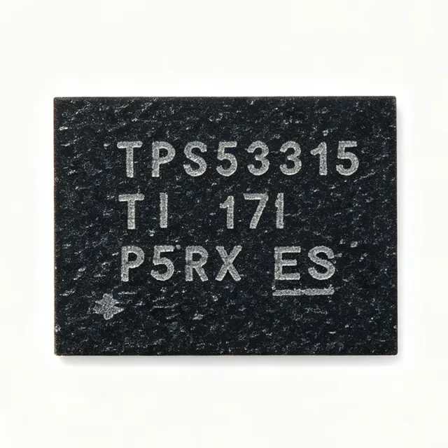
TPS53915RVER - 12A Sync Buck D-CAP3 Regulator | TI
MPN: TPS53915RVER ✓ Active| Qty | Unit Price | Extended |
|---|---|---|
| 1 | $6.1 | $6.10 |
| 10 | $5.49 | $54.90 |
| 100 | $4.72 | $472.00 |
| 500 | $4.05 | $2,025.00 |
| 1,000 | $3.48 | $3,480.00 |
TPS53915RVER Overview
A synchronous buck converter is a DC/DC switching regulator that uses two internal MOSFETs plus an inductor to step a higher input voltage down to a lower, well-regulated output. Within the power management hierarchy (regulator -> switching regulator -> SWIFT point-of-load converter), buck converters deliver high efficiency compared to linear regulators because power is transferred through inductive switching rather than dissipated as heat.
Key features include integrated 13.8-mOhm high-side and 5.9-mOhm low-side MOSFETs supporting 12-A continuous output current, PMBus-based configuration of voltage margining, soft-start time, power-on delay, VDD UVLO level and fault reporting, and an integrated boost switch for the high-side gate drive. The D-CAP3 adaptive on-time topology provides fast transient response with very low external component count, simplifying layouts in space-conscious systems.
Technically, the TPS53915 is trimmed at the factory to enable PMBus commands with a default switching frequency of 400 kHz. The device uses a current-consuming strategy for stability with low-ESR ceramic output capacitors and supports a wide duty cycle range, making it flexible across 5-V, 12-V and intermediate bus rails down to sub-1-V core voltages.
Typical applications include point-of-load power for DSPs, FPGAs and ASICs, industrial and enterprise server power rails, and telecom/datacom 12-V distributed power systems requiring fast transient response and high current density.
Design tip: ensure adequate PCB copper area on the exposed pad for heat dissipation at full 12-A load, and verify PMBus resistor straps or serial configuration choices against datasheet sequencing guidance before layout. Pricing shown is as of 2026-08-29.
Drop-in alternatives for TPS53915RVER — same package, pin-to-pin compatible. Different-package parts requiring PCB rework are excluded.
Quick Comparison Tool — Select alternative parts for side-by-side comparison:
TPS53622RSBT
✓ In Stock
$3.96 / Unit
View Datasheet →TPS53315
✓ In Stock
$3.52 / Unit
View Datasheet →TPS549A20RVER
📋 Reference alternative (not in catalog)
TPS53915EVER
📋 Reference alternative (not in catalog)
TPS53632GRSMR
📋 Reference alternative (not in catalog)
TPS53915RVER Maximum Ratings & Electrical Characteristics
| Topology | Synchronous Step-Down (Buck), D-CAP3 |
| Input Voltage Range | 1.5 V to 18 V |
| Bias Voltage Range | 4.5 V to 25 V |
| Output Voltage Range | 0.6 V to 5.5 V (adjustable) |
| Output Current | 12 A continuous |
| Reference Accuracy | 0.5% at 0.6 V |
| High-Side MOSFET Rds(on) | 13.8 mOhm (integrated) |
| Low-Side MOSFET Rds(on) | 5.9 mOhm (integrated) |
| Default Switching Frequency | 400 kHz (PMBus-trimmed default) |
| Control Mode | Adaptive On-Time D-CAP3 |
| Interface | PMBus (SWIFT voltage margining, soft-start, UVLO, fault reporting) |
| Number of Outputs | 1 |
| Package | 28-VFQFN Exposed Pad (VQFN-28) |
| Mounting Type | Surface Mount |
TPS53915RVER Pin Configuration
| Pin 1 | PVIN — Power-stage input voltage (1.5-18 V) |
| Pin 6 | SW — Switching node to inductor |
| Pin 10 | BOOT — High-side gate drive bootstrap (integrated boost switch) |
| Pin 13 | VDD — Bias supply input (4.5-25 V) |
| Pin 20 | GND — Ground reference / exposed pad |
| Pin 22 | FB — Feedback input for output regulation |
| Pin 27 | TRIM/TEST — Factory test and trim interface (may be grounded) |
| Pin 28 | TRIM/TEST — Factory test and trim interface (may be grounded) |
| Pin EP | Thermal Pad — Exposed pad, must be soldered to GND copper for thermal and electrical performance |
Typical Applications
TPS53915RVER is suitable for 6 applications: FPGA and ASIC Point-of-Load, Enterprise Server and Datacenter Power, Industrial Automation and Motor Drive Logic Rails, Telecom and Networking Equipment, Test and Measurement Instrumentation, Battery-Powered Portable Instruments.
FPGA and ASIC Point-of-Load
The TPS53915RVER's 12-A continuous output and 0.5% 0.6-V reference accuracy make it well suited to powering FPGA core rails that must stay within tight tolerance during heavy load steps. Its D-CAP3 adaptive on-time control reacts to transient events within microseconds, minimizing core-voltage droop without large output capacitor banks. Placed close to the FPGA with an appropriate inductor (typically 1-2 uH) and ceramic output capacitance, it converts a 12-V intermediate bus directly to 0.6-1.0-V core rails, reducing conversion stages and board space.
Recommended
Enterprise Server and Datacenter Power
In server and storage systems, dense point-of-load conversion from 12-V distributed rails is the dominant architecture. The TPS53915RVER's integrated 13.8/5.9-mOhm MOSFETs deliver high efficiency at 12 A, lowering heat load inside constrained chassis airflow. PMBus support enables voltage margining, sequencing and fault reporting managed by a system health controller, which is essential for hyperscale remote management. Its small VQFN-28 footprint with exposed pad allows compact multi-phase-rail designs per CPU or accelerator card while keeping component count and BOM cost low.
Recommended
Industrial Automation and Motor Drive Logic Rails
Industrial PLCs, drives and remote I/O modules commonly run 24-V or 12-V intermediate buses that must feed dense digital logic. The TPS53915RVER accepts a 4.5-25-V bias input, tolerating 24-V rail transients, while its D-CAP3 loop stays stable with low-ESR ceramic output capacitors that withstand industrial vibration and temperature. PMBus-configurable UVLO and soft-start allow designers to match power-up behavior to industrial sequencing requirements, and fault reporting simplifies diagnostics in unattended factory equipment, improving mean-time-to-repair on production lines.
Recommended
Telecom and Networking Equipment
Telecom rectifier and network switch boards distribute 12 V across backplanes and require many regulated lower-voltage rails with fast response. The TPS53915RVER's 1.5-18-V power input lets it convert directly from 12-V shelves, while the 400-kHz default switching frequency balances efficiency with small magnetics. Fast D-CAP3 transient response handles bursty traffic-dependent load changes in switch ASICs and network processors. PMBus margining lets system software verify supply health across thousands of deployed units, supporting predictive maintenance strategies in carrier-grade installations.
Recommended
Test and Measurement Instrumentation
Oscilloscopes, signal generators and automated test hardware embed numerous medium-current digital rails where low noise and accurate voltage matter. The TPS53915RVER's 0.5% reference accuracy and PMBus margining capability let instrument designers calibrate supply rails during production test. Its fast load transient response maintains regulation when measurement subsystems switch on and off, protecting sensitive analog front-end circuits sharing the board. The integrated MOSFETs and low external-component count also shrink power-supply area, leaving more PCB space for high-speed analog circuitry.
Recommended
Battery-Powered Portable Instruments
Portable test devices and field instruments running from multi-cell battery packs benefit from the TPS53915RVER's wide 1.5-18-V direct input, allowing operation as the pack discharges across its voltage range. High conversion efficiency from the integrated 5.9-mOhm low-side MOSFET extends runtime, while D-CAP3 control keeps efficiency high across light-load to full-load transitions typical of duty-cycled instruments. PMBus-configurable soft-start and power-on delay coordinate rail sequencing when the instrument wakes, protecting mixed-signal loads during battery hot-swap events.
Recommended
Recommended Products Summary
Engineering reference data for TPS53915RVER — comparison, design guidance, and compliance information.
Selection Guide
Comparison with Alternatives
| Parameter | This Product | TPS549A20RVER | TPS53915EVER | TPS53315 | TPS53632GRSMR |
|---|---|---|---|---|---|
| Package | VQFN-28 (RV) Exposed Pad | VQFN-28 - same | VQFN-28 - same | VQFN - different pinout | VQFN - different pinout |
| Brand | Texas Instruments | Texas Instruments | Texas Instruments | Texas Instruments | Texas Instruments |
| PMBus Interface | Yes (SWIFT) | Yes | Yes | D-CAP, pin-configured | Yes (SWIFT) |
Key Differentiators
- Integrated MOSFETs eliminate external power stage (vs TPS53632GRSMR)
- Fast transient response with low external count (vs TPS53315)
- True pin-compatible backup source within TI (vs TPS549A20RVER)
Design Notes
At full 12-A load with a 12-V input and 1-V output, converter losses concentrate in the integrated 13.8-mOhm high-side MOSFET during the on-time. The VQFN-28 exposed pad must be soldered to a solid ground plane with multiple thermal vias; follow the TI datasheet layout example. Measure junction temperature at maximum load and ambient to confirm margin against thermal shutdown.
Keep the SW node, BOOT and input capacitor loop as small as possible to minimize parasitic ringing and EMI. Place the ceramic input capacitors directly at PVIN with a low-inductance ground connection. Follow the TI TPS53915 datasheet EVM layout as the reference: short, wide traces for the power path and a dedicated quiet ground for FB and PMBus signals.
Pins 27-28 are the factory test-and-trim interface; grounding them is acceptable (they are grounded in TPS53513 sockets) but never drive them externally. Also remember the TPS53915 defaults to 400-kHz switching via factory trim when substituted into circuits designed for other SWIFT parts - verify loop compensation and inductor choice for that frequency before swapping devices.
Compliance Information
[DATA_NEEDED] Compliance status not stated in provided web data; verify RoHS/REACH on the TI product page.







