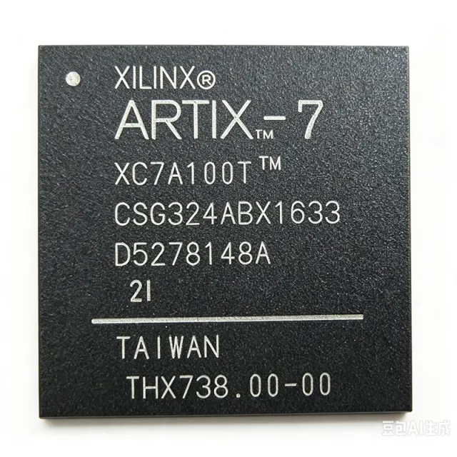
XC7A100T-1CSG324I-Q1 - Artix-7 FPGA, 101K Logic Cells | AMD
MPN: XC7A100T-1CSG324I-Q1 ✓ Active| Qty | Unit Price | Extended |
|---|---|---|
| 1 | $89.5 | $89.50 |
| 10 | $82.3 | $823.00 |
| 100 | $74.1 | $7,410.00 |
| 500 | $66.8 | $33,400.00 |
| 1,000 | $59.5 | $59,500.00 |
XC7A100T-1CSG324I-Q1 Overview
An FPGA (Field-Programmable Gate Array) is a semiconductor device containing configurable logic blocks and programmable interconnects, allowing designers to implement custom digital logic after manufacturing. Within the broader hierarchy, an FPGA is a type of programmable logic device (PLD), which falls under the category of integrated circuits (ICs) and ultimately semiconductors. The Artix-7 family specifically targets low-power, high-performance applications, balancing logic density with power efficiency.
Key features include 101,440 logic cells, 240 DSP48E1 slices for digital signal processing, and 4,860 Kb of block RAM. The device supports multiple I/O standards including LVCMOS, LVDS, and HSTL, and includes integrated PCIe blocks and GTP transceivers for high-speed serial communication. The -1 speed grade indicates a balanced performance level, while the I temperature grade supports operation from -40°C to +100°C (Tj).
The XC7A100T-1CSG324I-Q1 is built on AMD's 28nm process technology, offering a favorable balance of performance, power, and cost. The CSG324 package provides a compact footprint with 324 balls, enabling dense PCB layouts. The device includes configuration support via JTAG, SPI, and BPI interfaces, and features AES bitstream encryption for design security.
Typical applications include motor control in industrial automation, software-defined radio (SDR) for communications, medical imaging equipment, and automotive infotainment systems. The -Q1 suffix indicates automotive qualification, making it suitable for automotive applications requiring extended temperature ranges and reliability.
When designing with this FPGA, careful attention must be paid to power supply decoupling, with multiple 100nF capacitors placed near each power pin. The configuration interface should be selected based on the system boot requirements, with SPI flash being the most common choice for standalone operation.
This page synthesizes distributor pricing, drop-in alternatives, and practical design notes not found in the AMD datasheet, providing engineers with a comprehensive resource for design-in decisions.
Drop-in alternatives for XC7A100T-1CSG324I-Q1 — same package, pin-to-pin compatible. Different-package parts requiring PCB rework are excluded.
Quick Comparison Tool — Select alternative parts for side-by-side comparison:
XC7A100T-1CSG324I
✓ In Stock
$59.9 / Unit
View Datasheet →XC7A100T-2CSG324I
✓ In Stock
$105 / Unit
View Datasheet →XC7A100T-2CSG324I-Q1
📋 Reference alternative (not in catalog)
XC7A100T-1CSG324I-Q1 Maximum Ratings & Electrical Characteristics
| Logic Cells | 101,440 |
| Block RAM | 4,860 Kb |
| DSP Slices | 240 |
| User I/O Pins | 210 |
| Core Voltage | 1.0 V |
| Speed Grade | -1 |
| Temperature Grade | I (Industrial: -40°C to +100°C Tj) |
| Package | CSG324 (324-ball Chip Scale) |
| GTP Transceivers | 8 |
| PCIe Blocks | 1 |
| Configuration Interfaces | JTAG, SPI, BPI |
| Process Technology | 28 nm |
| Automotive Qualification | AEC-Q100 (Q1 suffix) |
| RoHS Status | Compliant |
| Mounting Type | Surface Mount |
XC7A100T-1CSG324I-Q1 Pin Configuration
| Pin A1 | IO_L1P_T0 — User I/O Bank 0, differential pair P |
| Pin A2 | IO_L1N_T0 — User I/O Bank 0, differential pair N |
| Pin B1 | IO_L2P_T0 — User I/O Bank 0, differential pair P |
| Pin B2 | IO_L2N_T0 — User I/O Bank 0, differential pair N |
| Pin C1 | VCCINT — Core voltage 1.0V |
| Pin C2 | GND — Ground |
| Pin D1 | IO_L3P_T0 — User I/O Bank 0, differential pair P |
| Pin D2 | IO_L3N_T0 — User I/O Bank 0, differential pair N |
| Pin E1 | VCCAUX — Auxiliary voltage 1.8V |
| Pin E2 | GND — Ground |
| Pin F1 | IO_L4P_T0 — User I/O Bank 0, differential pair P |
| Pin F2 | IO_L4N_T0 — User I/O Bank 0, differential pair N |
Typical Applications
XC7A100T-1CSG324I-Q1 is suitable for 6 applications: Automotive Motor Control, Software-Defined Radio (SDR), Medical Imaging, Industrial Automation, Automotive Infotainment, Aerospace and Defense.
Automotive Motor Control
The XC7A100T-1CSG324I-Q1 is ideal for automotive motor control systems such as electric power steering (EPS) and traction inverters. Its 240 DSP slices enable high-performance Field-Oriented Control (FOC) algorithms with fast current-loop processing. The device's 210 user I/O pins support multiple encoder interfaces (e.g., resolver, Hall effect) and PWM outputs for driving IGBT or MOSFET power stages. The automotive qualification (AEC-Q100) ensures reliable operation over the -40°C to +100°C junction temperature range, meeting the stringent reliability requirements of automotive environments. The GTP transceivers can be used for high-speed communication with external sensors or CAN-FD controllers, while the integrated PCIe block enables connection to automotive SoCs for centralized processing. The 4,860 Kb of block RAM provides ample storage for control algorithms and data buffering, and the 28nm process technology ensures low power dissipation, critical for thermally constrained automotive modules. Designers can leverage the Vivado Design Suite for implementing complex motor control algorithms, with the -Q1 variant providing the necessary automotive-grade reliability for safety-critical applications.
Recommended
Software-Defined Radio (SDR)
The XC7A100T-1CSG324I-Q1 is well-suited for software-defined radio (SDR) applications in defense and communications. Its 240 DSP slices provide the computational power for complex signal processing chains, including FFT, filtering, and modulation/demodulation. The 8 GTP transceivers support high-speed ADC/DAC interfaces up to 6.6 Gbps, enabling direct sampling of RF signals. The 101,440 logic cells allow implementation of multiple radio channels and protocols simultaneously, while the 4,860 Kb of block RAM buffers streaming data. The industrial temperature grade ensures operation in harsh environments, and the automotive qualification adds robustness for mobile or vehicular SDR systems. The PCIe block enables high-throughput data transfer to host processors, and the compact CSG324 package fits in space-constrained radio modules. Designers can use AMD's RFSoC tools and IP cores to accelerate development, with the -Q1 variant providing extended temperature reliability for field-deployed systems.
Recommended
Medical Imaging
The XC7A100T-1CSG324I-Q1 is used in medical imaging equipment such as ultrasound machines and CT scanners. Its 240 DSP slices accelerate image processing algorithms like beamforming and filtering, while the 101,440 logic cells implement complex control logic. The 4,860 Kb of block RAM stores image frames and intermediate results, and the 210 user I/O pins interface with image sensors and display controllers. The GTP transceivers enable high-speed data transfer from sensor arrays, and the PCIe block connects to host processors for image reconstruction. The industrial temperature grade ensures reliable operation in clinical environments, and the automotive qualification provides additional reliability for portable or mobile imaging systems. The compact CSG324 package allows integration into handheld ultrasound devices, and the 28nm process technology minimizes power consumption for battery-operated equipment. Designers can implement custom image processing pipelines using Vivado HLS, with the -Q1 variant offering extended temperature range for demanding clinical settings.
Recommended
Industrial Automation
The XC7A100T-1CSG324I-Q1 is a versatile choice for industrial automation, including PLCs, robotics, and machine vision. Its 101,440 logic cells implement complex control logic and communication protocols, while the 240 DSP slices handle real-time signal processing for sensor fusion. The 210 user I/O pins interface with industrial fieldbuses (EtherCAT, PROFINET) via external PHYs, and the GTP transceivers support high-speed industrial Ethernet. The 4,860 Kb of block RAM buffers process data, and the PCIe block connects to industrial PCs for HMI and data logging. The industrial temperature grade ensures operation in factory environments, and the automotive qualification adds robustness for harsh conditions. The compact CSG324 package fits in DIN-rail modules, and the 28nm process technology reduces power consumption for fanless designs. Designers can use AMD's industrial IP cores for EtherCAT and PROFINET, with the -Q1 variant providing extended reliability for 24/7 operation.
Recommended
Automotive Infotainment
The XC7A100T-1CSG324I-Q1 is used in automotive infotainment systems for video processing, display control, and connectivity. Its 101,440 logic cells implement video scalers, overlays, and GUI controllers, while the 240 DSP slices handle audio processing and noise cancellation. The 210 user I/O pins interface with LVDS displays, touch controllers, and camera sensors, and the GTP transceivers support high-speed USB or Ethernet connectivity. The 4,860 Kb of block RAM buffers video frames, and the PCIe block connects to automotive SoCs for application processing. The automotive qualification (AEC-Q100) ensures reliable operation over the -40°C to +100°C range, critical for in-vehicle electronics. The compact CSG324 package fits in head units and telematics boxes, and the 28nm process technology minimizes power consumption for battery-off scenarios. Designers can implement custom video pipelines using Vivado, with the -Q1 variant providing the necessary automotive-grade reliability for infotainment systems.
Recommended
Aerospace and Defense
The XC7A100T-1CSG324I-Q1 is suitable for aerospace and defense applications such as radar, electronic warfare, and secure communications. Its 240 DSP slices implement advanced signal processing algorithms for target detection and jamming, while the 101,440 logic cells handle complex control and encryption logic. The 8 GTP transceivers support high-speed data links for radar arrays and communication systems, and the PCIe block connects to mission computers. The 4,860 Kb of block RAM stores radar data and cryptographic keys, and the 210 user I/O pins interface with sensors and actuators. The industrial temperature grade ensures operation in extreme environments, and the automotive qualification adds robustness for ruggedized systems. The compact CSG324 package fits in avionics modules, and the 28nm process technology reduces power consumption for airborne platforms. Designers can implement secure bitstream encryption using AES, with the -Q1 variant providing extended temperature reliability for defense applications.
Recommended
Recommended Products Summary
Engineering reference data for XC7A100T-1CSG324I-Q1 — comparison, design guidance, and compliance information.
Selection Guide
Comparison with Alternatives
| Parameter | This Product | XC7A100T-1CSG324I | XC7A100T-2CSG324I-Q1 | XC7A100T-2CSG324I |
|---|---|---|---|---|
| Package | CSG324 | CSG324 - same | CSG324 - same | CSG324 - same |
| Speed Grade | -1 | -1 | -2 | -2 |
| Automotive Qualification | Yes (AEC-Q100) | No | Yes (AEC-Q100) | No |
| Logic Cells | 101,440 | 101,440 | 101,440 | 101,440 |
| Block RAM | 4,860 Kb | 4,860 Kb | 4,860 Kb | 4,860 Kb |
| DSP Slices | 240 | 240 | 240 | 240 |
| User I/O Pins | 210 | 210 | 210 | 210 |
| GTP Transceivers | 8 | 8 | 8 | 8 |
Key Differentiators
- Automotive qualification (AEC-Q100) (vs XC7A100T-1CSG324I)
- Balanced speed grade for power efficiency (vs XC7A100T-2CSG324I-Q1)
- Cost-optimized automotive solution (vs XC7A100T-2CSG324I-Q1)
Design Notes
The XC7A100T-1CSG324I-Q1 requires a 1.0V core supply (VCCINT), 1.8V auxiliary supply (VCCAUX), and 3.3V I/O supply (VCCO). Use a dedicated power management IC like the TI TPS54620 for the core supply to handle transient currents. Place 100nF ceramic capacitors near each power pin and a 10uF bulk capacitor per power rail. The total power consumption depends on logic utilization and clock frequency; for a typical design running at 200MHz, expect 1-2W dissipation.
The CSG324 package has a 0.8mm ball pitch, requiring careful PCB layout. Use 4-layer or more PCB with dedicated power and ground planes. Route high-speed GTP transceivers with controlled impedance (100 ohm differential) and keep trace lengths matched. Place decoupling capacitors on the bottom side of the PCB directly under the FPGA to minimize inductance. Follow AMD's PCB design guidelines in UG583 for optimal signal integrity.
Ensure the configuration voltage (VCCO_0) matches the configuration flash voltage (e.g., 3.3V for SPI flash). Do not leave unused I/O pins unconnected - set them to pull-up or pull-down in the Vivado constraints to avoid floating inputs. Verify the JTAG interface is properly terminated for production programming. For automotive applications, implement bitstream encryption using AES to protect IP, as the -Q1 variant supports this feature.
Compliance Information
RoHS compliant per AMD product page. AEC-Q100 qualified due to -Q1 suffix. REACH compliance assumed based on AMD's environmental policy.







