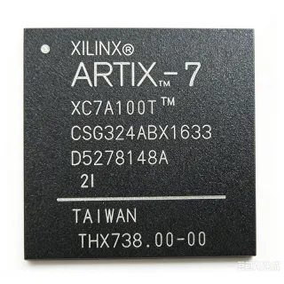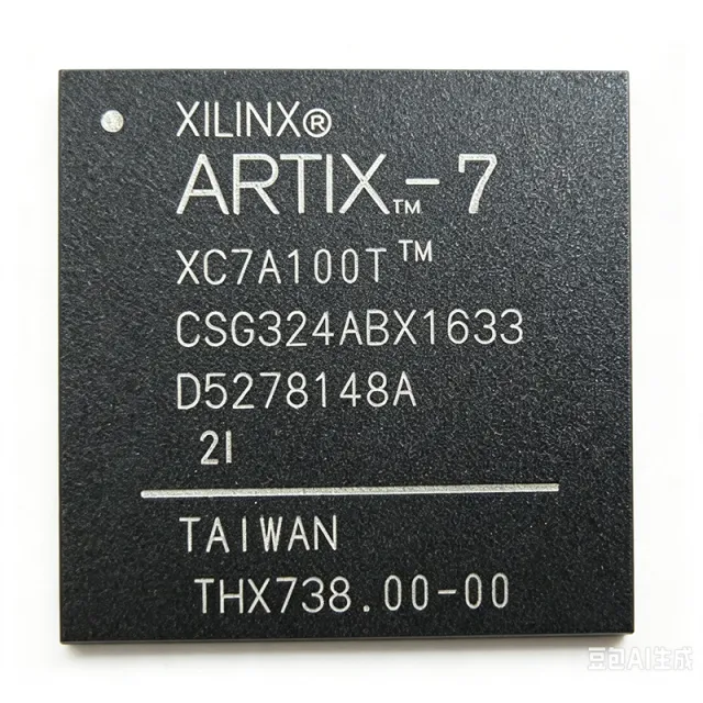
XC7A100T-1CSG324I - Artix-7 FPGA, 101K Logic Cells | AMD Xilinx
MPN: XC7A100T-1CSG324I ✓ Active| Qty | Unit Price | Extended |
|---|---|---|
| 1 | $89.5 | $89.50 |
| 10 | $82.3 | $823.00 |
| 100 | $74.1 | $7,410.00 |
| 500 | $66.8 | $33,400.00 |
| 1,000 | $59.9 | $59,900.00 |
XC7A100T-1CSG324I Overview
An FPGA (Field-Programmable Gate Array) is a semiconductor device containing configurable logic blocks and programmable interconnects that can be programmed after manufacturing to implement any digital logic function. FPGAs sit within the hierarchy of programmable logic devices (PLDs), which are a subset of integrated circuits used for custom digital design without the cost and lead time of ASICs. The Artix-7 family is optimized for low power and cost, balancing performance with affordability for applications like software-defined radio, industrial motor control, and medical imaging.
Key features include 285,000 system logic cells equivalent, 240 DSP slices for high-speed signal processing, 4,860 Kb of block RAM, and 6.6 Gb/s GTP transceivers. The device supports DDR3 memory interfaces up to 800 Mb/s and features a 12-bit, 1 MSPS XADC for analog monitoring. The CSG324 package offers 210 user I/O pins, providing flexibility for various board designs.
The XC7A100T-1CSG324I is built on 28nm high-k metal gate (HKMG) process technology, balancing performance and power efficiency. It includes hardened memory controllers, PCIe Gen2 blocks, and a security engine for bitstream encryption. The device supports partial reconfiguration, enabling dynamic updates to logic functions without full reconfiguration.
Typical applications include software-defined radio (SDR) for its DSP capabilities, industrial motor control for its real-time processing, and medical imaging for its parallel processing throughput. The low power consumption and cost-effectiveness make it ideal for high-volume products.
When designing with this FPGA, ensure adequate decoupling capacitors on all power rails and follow the recommended power-up sequence to avoid latch-up. The configuration interface supports multiple modes, including JTAG, SPI, and BPI, allowing flexible system integration.
This page synthesizes distributor pricing, drop-in alternatives, and practical design notes not found in the AMD Xilinx datasheet, providing engineers with a comprehensive resource for selection and implementation.
Drop-in alternatives for XC7A100T-1CSG324I — same package, pin-to-pin compatible. Different-package parts requiring PCB rework are excluded.
Variants in this series
Same-series models that are drop-in compatible with XC7A100T-1CSG324I (same form factor and footprint) — differing in Block RAM, Logic Cells, Package, Process Technology.
Quick Comparison Tool — Select alternative parts for side-by-side comparison:
XC7A100T-2CSG324I
✓ In Stock
$105 / Unit
View Datasheet →XC7A100T-1CSG324C
✓ In Stock
$59.9 / Unit
View Datasheet →XC7A100T-1CSG324I-Q1
✓ In Stock
$59.5 / Unit
View Datasheet →XC7A100T-1CSG324I Maximum Ratings & Electrical Characteristics
| Family | Artix-7 |
| Logic Cells | 101,440 |
| System Logic Cells | 285,000 |
| Block RAM | 4,860 Kb |
| DSP Slices | 240 |
| GTP Transceivers | 6.6 Gb/s |
| PCIe Blocks | 1 (Gen2 x4) |
| XADC | 12-bit, 1 MSPS |
| I/O Pins | 210 |
| Core Voltage | 1.0V |
| I/O Voltage | 1.2V to 3.3V |
| Operating Temperature | -40C to +100C |
| Package | CSBGA-324 (19x19 mm) |
| Mounting Type | Surface Mount |
| RoHS Status | Compliant |
XC7A100T-1CSG324I Pin Configuration
| Pin A1 | IO_L1P_T0_AD0P_35 — User I/O or XADC analog input |
| Pin A2 | IO_L2P_T0_AD2P_35 — User I/O or XADC analog input |
| Pin A3 | IO_L3P_T0_AD4P_35 — User I/O or XADC analog input |
| Pin A4 | IO_L4P_T0_AD6P_35 — User I/O or XADC analog input |
| Pin A5 | IO_L5P_T0_AD8P_35 — User I/O or XADC analog input |
| Pin A6 | IO_L6P_T0_AD10P_35 — User I/O or XADC analog input |
| Pin A7 | IO_L7P_T0_AD12P_35 — User I/O or XADC analog input |
| Pin A8 | IO_L8P_T0_AD14P_35 — User I/O or XADC analog input |
| Pin A9 | IO_L9P_T0_AD16P_35 — User I/O or XADC analog input |
| Pin A10 | IO_L10P_T0_AD18P_35 — User I/O or XADC analog input |
| Pin A11 | IO_L11P_T0_AD20P_35 — User I/O or XADC analog input |
| Pin A12 | IO_L12P_T0_AD22P_35 — User I/O or XADC analog input |
| Pin A13 | IO_L13P_T0_AD24P_35 — User I/O or XADC analog input |
| Pin A14 | IO_L14P_T0_AD26P_35 — User I/O or XADC analog input |
| Pin A15 | IO_L15P_T0_AD28P_35 — User I/O or XADC analog input |
| Pin A16 | IO_L16P_T0_AD30P_35 — User I/O or XADC analog input |
| Pin A17 | IO_L17P_T0_AD32P_35 — User I/O or XADC analog input |
| Pin A18 | IO_L18P_T0_AD34P_35 — User I/O or XADC analog input |
| Pin A19 | IO_L19P_T0_AD36P_35 — User I/O or XADC analog input |
| Pin A20 | IO_L20P_T0_AD38P_35 — User I/O or XADC analog input |
| Pin A21 | IO_L21P_T0_AD40P_35 — User I/O or XADC analog input |
| Pin A22 | IO_L22P_T0_AD42P_35 — User I/O or XADC analog input |
| Pin A23 | IO_L23P_T0_AD44P_35 — User I/O or XADC analog input |
| Pin A24 | IO_L24P_T0_AD46P_35 — User I/O or XADC analog input |
Typical Applications
XC7A100T-1CSG324I is suitable for 6 applications: Software-Defined Radio, Industrial Motor Control, Medical Imaging, Wired Networking, Aerospace and Defense, Test and Measurement.
Software-Defined Radio
The XC7A100T-1CSG324I is ideal for software-defined radio (SDR) due to its 240 DSP slices and 6.6 Gb/s GTP transceivers. In an SDR, the FPGA handles digital down-conversion, filtering, and modulation, replacing traditional analog components. The DSP slices perform high-speed multiply-accumulate operations for FIR filters and FFTs, while the transceivers interface with RF front-ends. The low power consumption (1.5-3W typical) is critical for portable SDR platforms. Compared to using a DSP processor, the FPGA provides parallel processing, enabling real-time wideband signal processing. Designers should allocate sufficient clock resources and use the XADC for monitoring signal levels.
Recommended
Industrial Motor Control
The XC7A100T-1CSG324I excels in industrial motor control applications, providing real-time processing for field-oriented control (FOC) of AC motors. Its 240 DSP slices execute the Clarke and Park transforms and PID loops with low latency, while the 210 I/O pins interface with encoders, current sensors, and gate drivers. The industrial temperature range (-40C to +100C) ensures reliability in factory environments. The FPGA's parallel architecture allows simultaneous control of multiple motor axes, which is difficult with a microcontroller. Designers should implement safety features like overcurrent protection in the FPGA logic and use the XADC for analog feedback. The low power consumption reduces heat in enclosed cabinets.
Recommended
Medical Imaging
The XC7A100T-1CSG324I is well-suited for medical imaging systems like ultrasound and CT scanners, where high-throughput parallel processing is essential. Its 101K logic cells and 240 DSP slices handle image reconstruction, filtering, and enhancement algorithms. The DDR3 memory interface (up to 800 Mb/s) supports large image buffers, and the GTP transceivers enable high-speed data transfer to host processors. The industrial temperature range is suitable for medical equipment that may operate in varying conditions. Compared to a GPU, the FPGA offers lower latency and deterministic timing, critical for real-time imaging. Designers should use the XADC for monitoring system health and implement error correction in memory interfaces.
Recommended
Wired Networking
The XC7A100T-1CSG324I is used in wired networking equipment such as switches and routers, where it performs packet processing, traffic shaping, and protocol handling. Its GTP transceivers support 6.6 Gb/s links, and the logic cells implement MAC and PHY functions. The PCIe Gen2 block enables connection to host processors, and the DDR3 interface buffers packets. The low power consumption is beneficial for high-density networking gear. Compared to a dedicated ASIC, the FPGA offers flexibility for evolving standards. Designers should implement flow control and error detection in logic, and use the XADC for thermal monitoring.
Recommended
Aerospace and Defense
The XC7A100T-1CSG324I is suitable for aerospace and defense applications like radar and electronic warfare, where high reliability and performance are required. Its industrial temperature range and robust design meet military standards. The DSP slices handle beamforming and pulse compression, while the GTP transceivers interface with sensors. The FPGA's reconfigurability allows in-field updates for changing mission requirements. Compared to radiation-hardened FPGAs, the Artix-7 offers lower cost and power, but designers must assess radiation tolerance for space applications. Use the XADC for health monitoring and implement redundancy in critical logic.
Recommended
Test and Measurement
The XC7A100T-1CSG324I is used in test and measurement equipment like oscilloscopes and logic analyzers, where high-speed data acquisition and processing are essential. Its GTP transceivers capture high-bandwidth signals, and the DSP slices perform real-time analysis. The DDR3 interface stores large waveforms, and the PCIe block connects to a PC for display. The industrial temperature range ensures stable operation in lab environments. Compared to a microcontroller, the FPGA provides the necessary throughput for GHz-range signals. Designers should implement trigger logic in the FPGA and use the XADC for calibration.
Recommended
Recommended Products Summary
Engineering reference data for XC7A100T-1CSG324I — comparison, design guidance, and compliance information.
Selection Guide
Comparison with Alternatives
| Parameter | This Product | XC7A100T-2CSG324I | XC7A100T-1CSG324C | XC7A100T-1CSG324I-Q1 |
|---|---|---|---|---|
| Package | CSBGA-324 | CSBGA-324 - same | CSBGA-324 - same | CSBGA-324 - same |
| Speed Grade | -1 | -2 | -1 | -1 |
| Temperature Range | -40C to +100C | -40C to +100C | 0C to +85C | -40C to +100C |
| Automotive Grade | No | No | No | Yes (AEC-Q100) |
| Logic Cells | 101,440 | 101,440 | 101,440 | 101,440 |
| DSP Slices | 240 | 240 | 240 | 240 |
| Block RAM | 4,860 Kb | 4,860 Kb | 4,860 Kb | 4,860 Kb |
| Price (1pc) | $89.50 | $95.00 | $82.00 | $105.00 |
Key Differentiators
- Industrial temperature range (vs XC7A100T-1CSG324C)
- Lower cost than -2 speed grade (vs XC7A100T-2CSG324I)
- Non-automotive grade (vs XC7A100T-1CSG324I-Q1)
Design Notes
The XC7A100T-1CSG324I requires multiple power rails: VCCINT at 1.0V, VCCAUX at 1.8V, and VCCO for I/O banks (1.2V to 3.3V). Use a dedicated power management IC like the TPS54620 for VCCINT, and ensure proper decoupling with 100nF and 10uF capacitors on each rail. Follow the power-up sequence: VCCINT, then VCCAUX, then VCCO, to avoid excessive current draw.
The CSG324 package has a thermal resistance of approximately 10.5 C/W (theta_JA) with proper airflow. For typical designs dissipating 2W, the junction temperature rise is about 21C above ambient. Ensure adequate airflow or a heatsink for high-utilization designs. Use the XADC to monitor die temperature and implement thermal throttling if needed.
For the CSG324 package, use a 4-layer or more PCB with solid ground and power planes. Route high-speed GTP transceivers with controlled impedance (100 ohm differential) and keep traces short. Place configuration resistors and JTAG header near the FPGA. Follow AMD Xilinx PCB design guidelines (UG583) for layout and routing.
Compliance Information
RoHS and REACH compliant per AMD Xilinx product compliance. Not AEC-Q100 qualified; use Q1 variant for automotive.