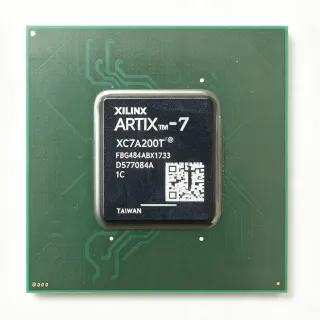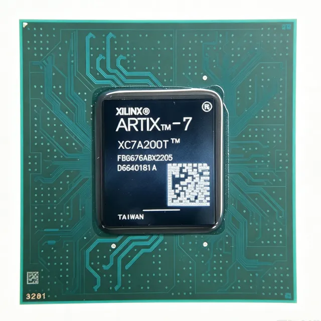
XC7A200T-3FBG676I - Artix-7 FPGA, 740K Logic Cells | AMD
MPN: XC7A200T-3FBG676I ✓ Active| Qty | Unit Price | Extended |
|---|---|---|
| 1 | $495 | $495.00 |
| 10 | $465 | $4,650.00 |
| 100 | $435 | $43,500.00 |
| 500 | $410 | $205,000.00 |
| 1,000 | $390 | $390,000.00 |
XC7A200T-3FBG676I Overview
An FPGA (Field-Programmable Gate Array) is an integrated circuit that can be configured by the customer after manufacturing to implement any digital logic function. FPGAs sit between ASICs (application-specific) and microprocessors (fixed instruction set) in the design hierarchy, offering reconfigurability and parallel processing. The Artix-7 family is optimized for high-performance, low-power applications, balancing logic density, DSP capability, and I/O flexibility.
Key features include 740K logic cells, 13.3 Mb of Block RAM, 740 DSP slices, and support for PCIe Gen2, Gigabit transceivers, and DDR3 memory interfaces. The -3 speed grade provides the highest performance in the Artix-7 family, with 6.6 Gb/s transceivers and 550 MHz clocking. The industrial temperature grade (-I) supports operation from -40C to +100C, making it suitable for harsh environments.
The XC7A200T-3FBG676I is built on 28nm process technology, offering a balance of performance and power efficiency. It includes hardened memory controllers for DDR3, and configurable logic blocks with 6-input LUTs. The device supports partial reconfiguration and has built-in analog-to-digital converter (XADC) for system monitoring.
Typical applications include software-defined radio, medical imaging, industrial motor control, and high-performance computing acceleration. The high DSP count and transceiver speed make it ideal for signal processing and high-throughput data paths.
When designing with this FPGA, ensure adequate decoupling capacitors on all power rails and follow the recommended power-up sequence. The configuration bitstream can be stored in external SPI flash or loaded via JTAG. Thermal management is critical at high utilization; use the exposed pad and proper airflow.
This page synthesizes distributor pricing, drop-in alternatives, and practical design notes not found in the AMD datasheet, providing a comprehensive resource for engineers evaluating the XC7A200T-3FBG676I.
Drop-in alternatives for XC7A200T-3FBG676I — same package, pin-to-pin compatible. Different-package parts requiring PCB rework are excluded.
Quick Comparison Tool — Select alternative parts for side-by-side comparison:
XC7A200T-2FBG676I
✓ In Stock
$100 / Unit
View Datasheet →XC7A200T-1FBG676I
✓ In Stock
$390 / Unit
View Datasheet →XC7A200T-3FBG676C
📋 Reference alternative (not in catalog)
XC7A200T-3FBG676I Maximum Ratings & Electrical Characteristics
| Family | Artix-7 |
| Logic Cells | 740K |
| Block RAM | 13.3 Mb |
| DSP Slices | 740 |
| Speed Grade | -3 |
| Temperature Grade | Industrial (-40C to +100C) |
| Package | FCBGA-676 (FBG676) |
| Core Voltage | 1.0V |
| I/O Voltage | 1.2V to 3.3V |
| GTX Transceivers | 16 (up to 6.6 Gb/s) |
| PCIe Blocks | 1 (Gen2 x4) |
| Memory Controllers | 2 (DDR3) |
| XADC | 1 (12-bit) |
| Configuration | SRAM-based |
| Process Technology | 28nm |
| RoHS Status | Compliant |
XC7A200T-3FBG676I Pin Configuration
| Pin A1 | IO_L1P_T0 — User I/O differential pair P |
| Pin A2 | IO_L1N_T0 — User I/O differential pair N |
| Pin B1 | GND — Ground |
| Pin B2 | VCCINT — Core voltage 1.0V |
| Pin C1 | IO_L2P_T0 — User I/O differential pair P |
| Pin C2 | IO_L2N_T0 — User I/O differential pair N |
| Pin D1 | VCCAUX — Auxiliary voltage 1.8V |
| Pin D2 | GND — Ground |
| Pin E1 | IO_L3P_T0 — User I/O differential pair P |
| Pin E2 | IO_L3N_T0 — User I/O differential pair N |
| Pin F1 | VCCIO_0 — I/O bank 0 voltage |
| Pin F2 | GND — Ground |
| Pin G1 | IO_L4P_T0 — User I/O differential pair P |
| Pin G2 | IO_L4N_T0 — User I/O differential pair N |
| Pin H1 | GND — Ground |
| Pin H2 | VCCINT — Core voltage 1.0V |
Typical Applications
XC7A200T-3FBG676I is suitable for 6 applications: Software-Defined Radio, Medical Imaging, Industrial Motor Control, High-Performance Computing Acceleration, Aerospace and Defense, Video and Image Processing.
Software-Defined Radio
The XC7A200T-3FBG676I is ideal for software-defined radio (SDR) due to its 740 DSP slices and 16 high-speed transceivers. In an SDR, the FPGA performs digital down/up conversion, filtering, and modulation/demodulation. The DSP slices handle complex multiply-accumulate operations at high throughput, while the transceivers interface with RF front-ends at up to 6.6 Gb/s. The Block RAM provides buffering for continuous data streams. The -3 speed grade ensures the FPGA can keep up with wideband signals, and the industrial temperature range allows deployment in field environments. Designers can implement multiple channels in parallel, leveraging the FPGA's parallel processing capability. Power consumption is manageable with proper clock gating and resource utilization. The XADC can monitor system health, and the PCIe block enables connection to a host processor for control and data transfer. Overall, the XC7A200T-3FBG676I provides the performance and flexibility required for advanced SDR systems.
Recommended
Medical Imaging
The XC7A200T-3FBG676I is well-suited for medical imaging systems such as ultrasound and CT scanners. These systems require high-speed data acquisition and real-time image processing. The FPGA's 740 DSP slices can implement filtering, beamforming, and image enhancement algorithms. The 13.3 Mb Block RAM stores image frames and intermediate results. High-speed transceivers interface with analog-to-digital converters (ADCs) and image sensors. The -3 speed grade ensures low latency processing, critical for real-time imaging. The industrial temperature range allows operation in clinical environments. The PCIe block connects to a host computer for display and storage. The XADC can monitor temperature and voltage for system reliability. With its high logic density, the FPGA can integrate multiple processing stages, reducing board space and power. The XC7A200T-3FBG676I enables compact, high-performance medical imaging devices.
Recommended
Industrial Motor Control
The XC7A200T-3FBG676I is used in industrial motor control for applications like robotics and CNC machines. The FPGA implements field-oriented control (FOC) algorithms for AC motors, requiring high-speed PWM generation and current sensing. The 740 DSP slices handle the complex math of FOC, including Clarke/Park transforms and PI controllers. The FPGA's parallel processing allows multiple motor axes to be controlled simultaneously. High-speed I/O interfaces with encoders and current sensors. The -3 speed grade ensures fast loop closure, improving dynamic response. The industrial temperature range is essential for factory environments. The XADC can monitor motor currents and temperatures for protection. The FPGA's reconfigurability allows firmware updates for different motor types. With its high logic density, the XC7A200T-3FBG676I can integrate communication interfaces like EtherCAT, reducing system cost. This FPGA provides the performance and reliability needed for advanced motor control.
Recommended
High-Performance Computing Acceleration
The XC7A200T-3FBG676I is used to accelerate compute-intensive workloads in data centers and scientific computing. The FPGA can implement custom accelerators for algorithms like cryptography, data compression, and machine learning inference. The 740 DSP slices provide high throughput for matrix operations. The 13.3 Mb Block RAM enables on-chip data caching, reducing memory latency. High-speed transceivers connect to host servers via PCIe or Ethernet. The -3 speed grade maximizes compute throughput. The FPGA's reconfigurability allows dynamic adaptation to different workloads. The PCIe block provides a high-bandwidth interface to the host CPU. The XADC monitors power and temperature for reliable operation. With its high logic density, the FPGA can implement multiple accelerators in parallel, achieving significant speedups over software. The XC7A200T-3FBG676I offers a flexible and efficient solution for accelerating diverse applications.
Recommended
Aerospace and Defense
The XC7A200T-3FBG676I is suitable for aerospace and defense applications such as radar, electronic warfare, and secure communications. These systems require high-performance signal processing and rugged reliability. The FPGA's 740 DSP slices handle pulse compression, beamforming, and FFTs. The high-speed transceivers interface with radar front-ends and communication links. The industrial temperature range (-40C to +100C) meets military specifications. The XADC monitors system health in harsh environments. The FPGA's reconfigurability allows secure key updates and waveform changes. The -3 speed grade ensures real-time processing of high-bandwidth signals. The PCIe block enables integration with mission computers. With its high logic density, the FPGA can implement multiple functions, reducing size, weight, and power (SWaP). The XC7A200T-3FBG676I provides the performance and reliability required for defense systems.
Recommended
Video and Image Processing
The XC7A200T-3FBG676I is used in video and image processing systems like broadcast equipment, surveillance cameras, and machine vision. The FPGA implements video scaling, color space conversion, and compression algorithms. The 740 DSP slices handle pixel processing at high throughput. The 13.3 Mb Block RAM stores line buffers and frame data. High-speed transceivers interface with video sources and displays via standards like HDMI and DisplayPort. The -3 speed grade ensures real-time processing of 4K video. The industrial temperature range allows outdoor surveillance use. The PCIe block connects to host processors for video analytics. The XADC monitors temperature for reliable operation. With its high logic density, the FPGA can integrate multiple video channels, reducing system cost. The XC7A200T-3FBG676I provides the performance and flexibility for advanced video processing.
Recommended
Recommended Products Summary
Engineering reference data for XC7A200T-3FBG676I — comparison, design guidance, and compliance information.
Selection Guide
Comparison with Alternatives
| Parameter | This Product | XC7A200T-2FBG676I | XC7A200T-1FBG676I | XC7A200T-3FBG676C |
|---|---|---|---|---|
| Package | FCBGA-676 (FBG676) | FCBGA-676 (FBG676) - same | FCBGA-676 (FBG676) - same | FCBGA-676 (FBG676) - same |
| Speed Grade | -3 | -2 | -1 | -3 |
| Temperature Grade | Industrial (-40C to +100C) | Industrial (-40C to +100C) | Industrial (-40C to +100C) | Commercial (0C to +85C) |
| Logic Cells | 740K | 740K | 740K | 740K |
| Block RAM | 13.3 Mb | 13.3 Mb | 13.3 Mb | 13.3 Mb |
| DSP Slices | 740 | 740 | 740 | 740 |
| GTX Transceivers | 16 (up to 6.6 Gb/s) | 16 (up to 6.6 Gb/s) | 16 (up to 6.6 Gb/s) | 16 (up to 6.6 Gb/s) |
| Price (1 pc) | $495.00 | $450.00 | $420.00 | $480.00 |
Key Differentiators
- Highest speed grade in Artix-7 family (vs XC7A200T-2FBG676I)
- Industrial temperature range (vs XC7A200T-3FBG676C)
- Same package and pinout as other speed grades (vs XC7A200T-1FBG676I)
Design Notes
The XC7A200T-3FBG676I requires multiple power rails: VCCINT at 1.0V, VCCAUX at 1.8V, and VCCIO for each I/O bank (1.2V to 3.3V). Use a dedicated power management IC or DC-DC converters with proper sequencing. Ensure VCCINT is stable before configuration. Decouple each rail with 100nF and 10uF capacitors per pin group.
At high utilization, the XC7A200T-3FBG676I can dissipate over 10W. The FCBGA-676 package has a thermal resistance of about 8-10 C/W (theta_JA) with airflow. Use a heatsink or forced air cooling to keep junction temperature below 100C. The industrial grade allows up to 100C, but reliability improves with lower temperatures.
For high-speed transceivers, use controlled impedance traces (e.g., 100 ohm differential) and minimize via stubs. Place decoupling capacitors close to the FPGA power pins. Follow the PCB design guidelines in UG483 for Artix-7. Ensure adequate ground planes for return currents.
Compliance Information
RoHS compliant per AMD product page. Not AEC-Q100 qualified as it is an FPGA, not an automotive-grade component.