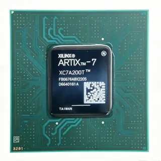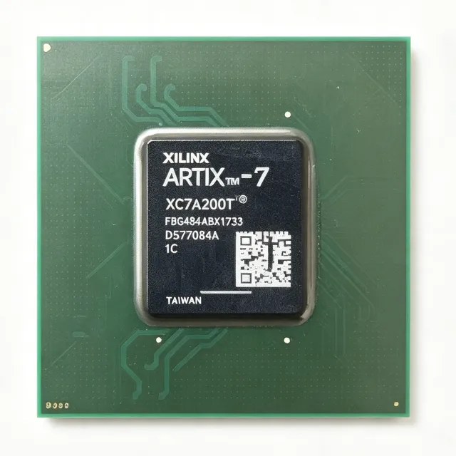
XC7A200T-1FBG676I - 740K Logic Cells FPGA | AMD Xilinx | FBG676
MPN: XC7A200T-1FBG676I ✓ Active| Qty | Unit Price | Extended |
|---|---|---|
| 1 | $495 | $495.00 |
| 10 | $465 | $4,650.00 |
| 100 | $435 | $43,500.00 |
| 500 | $410 | $205,000.00 |
| 1,000 | $390 | $390,000.00 |
XC7A200T-1FBG676I Overview
An FPGA (Field-Programmable Gate Array) is an integrated circuit that can be configured by the designer after manufacturing, offering reconfigurable logic blocks and programmable interconnects. FPGAs sit within the broader hierarchy of programmable logic devices (PLDs), which are a subset of digital integrated circuits. They provide a flexible alternative to ASICs, enabling rapid prototyping and hardware acceleration without the high NRE costs of custom silicon.
Key features include 740K logic cells, 365 DSP48E1 slices, 10.5 Mb of distributed RAM, and 13,140 Kb of Block RAM. The device supports up to 400 I/O pins with SelectIO technology, offering programmable I/O standards and speeds. It also includes integrated PCIe blocks, Gigabit Transceivers (GTX) for high-speed serial communication, and a XADC for analog-to-digital conversion, providing a comprehensive platform for complex digital systems.
The Artix-7 architecture is built on a 28nm high-k metal gate (HKMG) process, balancing performance and power efficiency. The device features a configurable logic block (CLB) structure with 6-input LUTs, dedicated carry chains, and flip-flops, enabling efficient implementation of complex logic functions. The DSP48E1 slices support high-speed arithmetic operations, while the Block RAM provides on-chip storage for data buffering and FIFO implementations.
Typical applications include software-defined radio (SDR), medical imaging, industrial motor control, and high-performance computing acceleration. The high logic density and DSP resources make it ideal for signal processing tasks, while the transceivers enable high-speed data communication in networking and broadcast equipment.
When designing with this FPGA, careful attention must be paid to power supply decoupling and thermal management. The device requires multiple supply rails (VCCINT, VCCAUX, VCCO) with proper sequencing, and the 676-ball BGA package demands a multi-layer PCB with adequate thermal vias for heat dissipation. This page synthesizes distributor pricing, drop-in alternatives, and practical design notes not found in the AMD datasheet.
Drop-in alternatives for XC7A200T-1FBG676I — same package, pin-to-pin compatible. Different-package parts requiring PCB rework are excluded.
Quick Comparison Tool — Select alternative parts for side-by-side comparison:
XC7A200T-2FBG676I
✓ In Stock
$100 / Unit
View Datasheet →XC7A200T-1FBG676C
📋 Reference alternative (not in catalog)
XC7A200T-1FBG676I Maximum Ratings & Electrical Characteristics
| Family | Artix-7 |
| Logic Cells | 740K |
| Logic Slices | 215,360 |
| Block RAM | 13,140 Kb |
| Distributed RAM | 10.5 Mb |
| DSP48E1 Slices | 365 |
| Maximum I/O Pins | 400 |
| Core Voltage (VCCINT) | 1.0 V |
| I/O Voltage (VCCO) | 1.2 V to 3.3 V |
| Package | FCBGA-676 (FBG676) |
| Operating Temperature | -40C to +100C (I grade) |
| Speed Grade | -1 |
| GTX Transceivers | 16 |
| PCIe Blocks | 1 |
| XADC Blocks | 1 |
| RoHS Status | Compliant |
XC7A200T-1FBG676I Pin Configuration
| Pin A1 | IO_L1P_T0 — User I/O differential pair P |
| Pin A2 | IO_L1N_T0 — User I/O differential pair N |
| Pin B1 | IO_L2P_T0 — User I/O differential pair P |
| Pin B2 | IO_L2N_T0 — User I/O differential pair N |
| Pin C1 | VCCINT — Core voltage 1.0V |
| Pin C2 | GND — Ground |
| Pin D1 | IO_L3P_T0 — User I/O differential pair P |
| Pin D2 | IO_L3N_T0 — User I/O differential pair N |
| Pin E1 | VCCAUX — Auxiliary voltage 1.8V |
| Pin E2 | GND — Ground |
| Pin F1 | IO_L4P_T0 — User I/O differential pair P |
| Pin F2 | IO_L4N_T0 — User I/O differential pair N |
Typical Applications
XC7A200T-1FBG676I is suitable for 6 applications: Software-Defined Radio (SDR), Medical Imaging, Industrial Motor Control, High-Performance Computing Acceleration, Broadcast Video Processing, Aerospace and Defense.
Software-Defined Radio (SDR)
The XC7A200T-1FBG676I is ideal for SDR platforms due to its high logic density and DSP resources. With 365 DSP48E1 slices, it can implement complex modulation/demodulation algorithms, channel filters, and FFT engines. The 16 GTX transceivers provide high-speed serial interfaces to connect to ADCs and DACs, enabling wideband signal processing. The XADC block allows on-chip monitoring of signal levels and temperature, enhancing system reliability. In a typical SDR, the FPGA handles baseband processing, digital up/down conversion, and protocol stack implementation, offloading the host processor. The industrial temperature grade ensures operation in field-deployed environments.
Recommended
Medical Imaging
The XC7A200T-1FBG676I is well-suited for medical imaging systems such as ultrasound and CT scanners, where high-speed signal processing and data throughput are critical. Its 740K logic cells enable implementation of image reconstruction algorithms, filtering, and beamforming. The 13,140 Kb of Block RAM provides ample storage for image frames and intermediate data. The 400 I/O pins interface with sensor arrays and memory devices, while the GTX transceivers can stream processed images to display systems. The industrial temperature grade ensures reliable operation in clinical environments. The FPGA's reconfigurability allows for algorithm updates without hardware changes, extending product lifespan.
Recommended
Industrial Motor Control
The XC7A200T-1FBG676I excels in industrial motor control applications, providing high-performance processing for field-oriented control (FOC) algorithms. Its 365 DSP48E1 slices handle the complex mathematical operations required for real-time current and speed control loops. The FPGA's deterministic timing ensures precise PWM generation for inverter stages, reducing torque ripple and improving efficiency. With 400 I/O pins, it can interface with encoders, current sensors, and gate drivers. The industrial temperature grade (-40C to +100C) makes it suitable for factory floor environments. The reconfigurable nature allows for customization of control algorithms for different motor types and power ratings.
Recommended
High-Performance Computing Acceleration
The XC7A200T-1FBG676I can accelerate compute-intensive workloads in data centers and scientific computing. Its 740K logic cells and 365 DSP slices enable implementation of custom arithmetic units, such as FFTs, matrix multipliers, and cryptographic engines. The 16 GTX transceivers provide high-bandwidth connectivity to host processors or other FPGAs, enabling scalable acceleration platforms. The Block RAM and distributed RAM offer on-chip data storage, reducing memory latency. The FPGA's parallel processing capability delivers significant speedups over CPU-only implementations for specific algorithms. The industrial temperature grade ensures reliable operation in server environments.
Recommended
Broadcast Video Processing
The XC7A200T-1FBG676I is used in broadcast video equipment for real-time processing of high-definition video streams. Its high logic density supports video codecs, scaling, color space conversion, and frame rate conversion. The 13,140 Kb of Block RAM is sufficient for line buffers and frame storage. The GTX transceivers can handle SDI (Serial Digital Interface) signals at 3G/6G/12G rates, enabling direct connection to broadcast infrastructure. The 400 I/O pins interface with video codec chips and external memory. The industrial temperature grade ensures reliable operation in broadcast facilities. The FPGA's reconfigurability allows for support of evolving video standards.
Recommended
Aerospace and Defense
The XC7A200T-1FBG676I is suitable for aerospace and defense applications such as radar, electronic warfare, and secure communications. Its industrial temperature grade and high reliability make it suitable for harsh environments. The 365 DSP slices enable advanced signal processing for radar pulse compression and beamforming. The 16 GTX transceivers support high-speed data links for sensor fusion. The FPGA's reconfigurability allows for in-field updates of encryption algorithms and waveforms. The XADC block provides on-chip monitoring for health management. The device's high logic density supports complex system-on-chip designs, reducing board space and power.
Recommended
Recommended Products Summary
Engineering reference data for XC7A200T-1FBG676I — comparison, design guidance, and compliance information.
Selection Guide
Comparison with Alternatives
| Parameter | This Product | XC7A200T-2FBG676I | XC7A200T-1FBG676C | XC7A200T-1FBG676I |
|---|---|---|---|---|
| Package | FCBGA-676 (FBG676) | FCBGA-676 (FBG676) - same | FCBGA-676 (FBG676) - same | FCBGA-676 (FBG676) - same |
| Speed Grade | -1 | -2 | -1 | -1 |
| Temperature Grade | Industrial (-40C to +100C) | Industrial (-40C to +100C) | Commercial (0C to +85C) | Industrial (-40C to +100C) |
| Logic Cells | 740K | 740K | 740K | 740K |
| Block RAM | 13,140 Kb | 13,140 Kb | 13,140 Kb | 13,140 Kb |
| DSP Slices | 365 | 365 | 365 | 365 |
| GTX Transceivers | 16 | 16 | 16 | 16 |
| Price (1 pc) | $495.00 | $520.00 | $450.00 | $495.00 |
Key Differentiators
- Higher speed grade option (vs XC7A200T-1FBG676I)
- Industrial temperature grade (vs XC7A200T-1FBG676C)
- Identical part for redundancy (vs XC7A200T-1FBG676I)
Design Notes
The XC7A200T-1FBG676I requires multiple power rails: VCCINT at 1.0V, VCCAUX at 1.8V, and VCCO depending on I/O banks (1.2V to 3.3V). Use low-dropout regulators or DC-DC converters with adequate current capability. Decouple each rail with 100nF and 10uF capacitors placed close to the FPGA pins. Follow the power sequencing requirements in the datasheet to avoid damage.
The FBG676 package can dissipate significant heat under heavy utilization. Use a thermal analysis tool to estimate junction temperature. Ensure adequate airflow or attach a heatsink to the top of the package. Provide thermal vias under the package to conduct heat to the PCB ground plane. The maximum junction temperature is 125C for industrial grade.
For the 676-ball BGA, use a multi-layer PCB with at least 8 layers for signal routing and power planes. Follow the PCB design guidelines in UG483 (Artix-7 FPGA PCB Design Guide). Ensure proper pad size and solder mask openings for reliable soldering. Use Xilinx's pinout files to assign I/O pins to minimize routing congestion.
Compliance Information
RoHS compliant per AMD Xilinx product documentation. AEC-Q100 not applicable for FPGA devices. Halogen-free status not specified in available data.