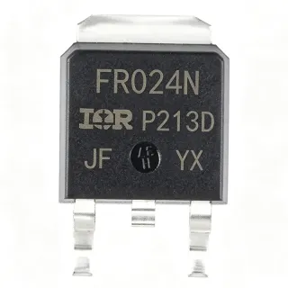
IRLR3636TRLPBF - 60V 99A N-Ch IR MOSFET, DPAK | Infineon
MPN: IRLR3636TRLPBF ✓ Hoạt độngIRLR3636TRLPBF Tóm tắt
A power MOSFET is a voltage-controlled semiconductor switch that uses an insulated gate to modulate current flow between drain and source terminals. The IRLR3636TRLPBF belongs to the N-channel enhancement-mode MOSFET family, where applying a positive gate-source voltage creates an inversion layer that conducts current. As part of the broader MOSFET → power transistor → discrete semiconductor → semiconductor taxonomy, it sits in the voltage-regulator/synchronous-rectification segment of power electronics where low RDS(on) and fast switching directly impact efficiency.
Key features of the IRLR3636TRLPBF include 6.8 mΩ maximum RDS(on), 99 A peak ID, logic-level gate threshold (VGS(th) around 1.0-2.5 V), avalanche-rated body diode, and 33 nC total gate charge. The low on-resistance minimises conduction losses, while the small QG reduces switching losses at high frequencies, collectively improving system efficiency in SMPS and motor-drive applications.
The device uses Infineon's advanced IR process technology, combining a trench MOSFET architecture with a ruggedised die layout. This produces a low figure-of-merit (FOM = RDS(on) × QG) and robust avalanche capability. The DPAK package provides a low thermal resistance path via its exposed drain tab, which doubles as the mounting surface for heat-sinking to the PCB copper pour.
Typical applications include DC motor drives, high-efficiency synchronous rectification in switch-mode power supplies (SMPS), uninterruptible power supplies (UPS), and high-speed power switching in hard-switched topologies. The logic-level gate makes it directly compatible with 5 V microcontroller outputs without a dedicated gate driver in lower-power circuits.
When designing with this MOSFET, ensure that the gate drive voltage stays within the absolute-maximum VGS rating of ±20 V (or ±16 V per some datasheet sources). PCB layout should minimise the source-inductance loop; place the gate driver physically close to the gate pin and use a Kelvin-source connection where possible.
This page synthesises distributor pricing, drop-in alternatives, and practical design notes that go beyond the manufacturer datasheet alone, giving engineers a single reference for selecting and qualifying this part.
Bộ thay thế dễ dàng lắp đặt cho IRLR3636TRLPBF — cùng gói, chân-to-chân tương thích. Các bộ phận yêu cầu hàn PCB bị loại trừ.
Các biến thể trong loạt này
Các mẫu cùng loạt có thể lắp đặt dễ dàng tương thích với IRLR3636TRLPBF (cùng hình factor và footprint) — khác nhau ở Technology, Package, FET Type, Operating Temperature Range, Total Gate Charge (Qg).
IRLR3636PBF
✅ Drop-In📋 Tham chiếu thay thế (không có trong danh mục)
IRLR3636TRPBF
✅ Drop-InLiên hệ để biết giá
Xem tài liệu →AUIRLR3636
✅ Drop-In📋 Tham chiếu thay thế (không có trong danh mục)
IRLR3410TRPBF
✅ Drop-InLiên hệ để biết giá
Xem tài liệu →IRLR3114ZTRPBF
✅ Drop-InLiên hệ để biết giá
Xem tài liệu →IRLR2905TRPBF
✅ Drop-InLiên hệ để biết giá
Xem tài liệu →IRLR3636TRLPBF Tỷ lệ tối đa & tính chất điện
| FET Type | N-Channel MOSFET |
| Technology | IR HEXFET® (IR MOSFET™) |
| Drain-to-Source Voltage (VDS) | 60 V |
| Continuous Drain Current (ID, TC=25°C) | 50 A |
| RDS(on) Max @ VGS=10V | 6.8 mΩ |
| Gate-to-Source Voltage (VGS) Max | ±20 V |
| Gate Threshold Voltage (VGS(th)) | 1.0 V to 2.5 V (logic-level) |
| Total Gate Charge (QG) | 33 nC |
| Power Dissipation (PD, TC=25°C) | 143 W |
| Khoảng nhiệt độ hoạt động | -55 °C to +175 °C (TJ) |
| Hộp | TO-252AA (DPAK) |
| Kiểu lắp đặt | Surface Mount |
| Lead-Free / RoHS | Yes (PBF suffix) |
| Avalanche Rated | Yes (per Infineon datasheet family) |
Cấu hình chân IRLR3636TRLPBF
| Chân 1 | Gate — Gate drive input (logic-level, VGS(th) 1.0-2.5 V) |
| Chân 2 | Drain (Tab) — Drain output, internally connected to the mounting tab; tab is the primary thermal dissipation path |
| Chân 3 | Source — Source return, connect to system ground (or low-side shunt) |
Khu vực hoạt động an toàn (DC, TC=25°C)
Ứng dụng tiêu biểu
IRLR3636TRLPBF phù hợp cho 6 Áp dụngs: DC Motor Drive (H-Bridge / Half-Bridge), Synchronous Rectification in SMPS, Uninterruptible Power Supply (UPS) Battery Switch, High-Side/Low-Side Power Switching in E-Bike / E-Scooter, Solar Charge Controller / Battery Management, Industrial Solenoid / Relay Driver.
DC Motor Drive (H-Bridge / Half-Bridge)
The IRLR3636TRLPBF is well-suited to 12-48 V brushed DC motor drive half-bridges and H-bridges. Its 60 V VDS rating provides adequate headroom for inductive flyback transients in 24 V and 36 V battery-powered systems, while the 6.8 mΩ RDS(on) at logic-level VGS minimises conduction loss during PWM operation at high duty cycle. The DPAK package's exposed drain tab ties directly to a copper pour, enabling continuous currents above 30 A without forced-air cooling. Designers should add a snubber or TVS clamp across the drain-source to absorb avalanche energy during motor commutation.
Được đề xuất
Synchronous Rectification in SMPS
As a synchronous rectifier on the secondary side of an isolated SMPS, the IRLR3636TRLPBF's low RDS(on) of 6.8 mΩ and 33 nC total gate charge deliver a figure-of-merit that approaches efficiency limits for 12 V output rails. Replacing Schottky diodes in 5 V to 12 V buck-derived converters reduces forward-conduction loss from ~0.5 V to a few mV at full load. The logic-level gate allows direct drive from a sync-rectifier controller IC such as the NCP4306. Engineers should observe the body-diode reverse-recovery characteristic when used in hard-switched topologies above 100 kHz.
Được đề xuất
Uninterruptible Power Supply (UPS) Battery Switch
In line-interactive and online UPS designs, the IRLR3636TRLPBF serves as the low-side disconnect switch between the battery bank and the DC bus, or as part of a bidirectional buck-boost converter for battery charging/discharging. Its 50 A continuous drain rating handles typical 1-2 kVA UPS battery currents with margin, and the 60 V VDS covers 48 V battery stacks including transient surges. The DPAK package enables compact PCB layouts in 1U rack-mounted UPS form factors. A pre-charge resistor plus NTC thermistor is recommended to limit inrush current at hot-plug events.
Được đề xuất
High-Side/Low-Side Power Switching in E-Bike / E-Scooter
The IRLR3636TRLPBF functions as the low-side PWM switch or synchronous FET in 24-36 V e-bike controller boards. Its logic-level gate drive allows direct connection to a 3.3 V or 5 V MCU PWM output through a small gate resistor, eliminating a discrete gate driver in cost-sensitive designs. The 6.8 mΩ RDS(on) keeps conduction loss manageable for motor currents up to 25 A continuous, while the rugged DPAK package withstands the vibration and thermal cycling typical of personal-electric-vehicle duty profiles.
Được đề xuất
Solar Charge Controller / Battery Management
In MPPT or PWM solar charge controllers for off-grid photovoltaic systems, the IRLR3636TRLPBF operates as the main switching element in the buck converter between the PV panel (open-circuit up to ~45 V in 24 V systems) and the battery bus. Its 60 V VDS handles 24 V panel Voc with margin, while the low RDS(on) reduces thermal stress during continuous 30-40 A charge currents. The part's avalanche rating also tolerates the inductive ringing from long PV-cable inductance during MPPT step changes.
Được đề xuất
Industrial Solenoid / Relay Driver
The IRLR3636TRLPBF is a robust low-side driver for 24 V industrial solenoid valves, pneumatic actuators, and relay coils. Each FET can switch several amps of inductive load current with logic-level control from a PLC output or industrial microcontroller. The 60 V VDS comfortably clamps the inductive kickback when combined with a flyback diode or TVS clamp, and the DPAK package dissipates the average coil current without a heatsink in many cases. For multi-channel solenoid banks, paralleling multiple IRLR3636TRLPBF devices shares current and reduces per-channel RDS(on).
Được đề xuất
Tóm tắt các sản phẩm được đề xuất
Dữ liệu tham khảo kỹ thuật cho IRLR3636TRLPBF — so sánh, hướng dẫn thiết kế và thông tin tuân thủ.
Hướng dẫn chọn lựa
So sánh với các sản phẩm thay thế
| Tham số | Sản phẩm này | IRLR3636PBF | AUIRLR3636 | IRLR3410TRPBF | IRLR3114ZTRPBF |
|---|---|---|---|---|---|
| Brand | Infineon Technologies | Infineon Technologies | Infineon Technologies | Infineon Technologies | Infineon Technologies |
| Package | TO-252AA (DPAK) | TO-252AA (DPAK) - same | TO-252AA (DPAK) - same | TO-252AA (DPAK) - same | TO-252AA (DPAK) - same |
| Drain-Source Voltage (VDS) | 60 V | 60 V | 60 V | 100 V | 40 V |
| Continuous Drain Current (ID, TC=25°C) | 50 A | 50 A | 50 A | 30 A | 40 A |
| RDS(on) Max @ VGS=10V | 6.8 mΩ | 6.8 mΩ | 6.8 mΩ | 28 mΩ | 3.2 mΩ |
| Gate Threshold (VGS(th)) | 1.0 V to 2.5 V (logic-level) | 1.0 V to 2.5 V | 1.0 V to 2.5 V | 1.0 V to 2.5 V | 1.0 V to 2.5 V |
| Total Gate Charge (QG) | 33 nC | 33 nC | 33 nC | 48 nC | 24 nC |
| Power Dissipation (PD) | 143 W | 143 W | 143 W | 120 W | 130 W |
| Automotive Grade | No (industrial) | No | Yes (AEC-Q101) | No | No |
Bảo phân biệt quan trọng
- Lower RDS(on) than higher-voltage family parts (vsIRLR3410TRPBF)
- Logic-level gate drive compatible with 5V MCU (vsIRLR3114ZTRPBF)
- Automotive-qualified option available on same die (vsAUIRLR3636)
Ghi chú thiết kế
Estimated: At continuous drain current of 30 A with RDS(on) = 6.8 mΩ, conduction loss is approximately P = I² × RDS(on) = 30² × 0.0068 ≈ 6.1 W. The TO-252 DPAK package has theta_JA ≈ 50 °C/W on a 1 oz single-sided 1 sq-inch copper pad, giving a junction temperature rise of ~305 °C - clearly above the 175 °C limit. For 30 A continuous operation, the design must use a minimum 4 sq-inch copper pour on both sides of the PCB, or attach an external heatsink. Derate to ~15-20 A continuous without a heatsink on a typical 2-layer FR4 board.
The DPAK drain tab doubles as the thermal pad and must be soldered to a substantial copper pour for heat dissipation. Recommended land pattern per IPC-7351: drain pad 6.5 mm × 5.5 mm minimum, gate and source pads 1.5 mm × 1.0 mm with 0.5 mm pitch. Use thermal vias (0.3 mm diameter, 1 mm pitch) under the drain pad to inner copper planes. Gate-drive traces should be kept short (<10 mm) to minimise gate-loop inductance and prevent ringing during fast switching edges.
Three common pitfalls with this part: (1) Do not exceed VGS absolute maximum of ±20 V; use a gate-source Zener clamp (e.g. 15 V) when driving from a 12 V or higher rail. (2) The body diode reverse-recovery (Qrr) is significant in hard-switched topologies above 100 kHz - consider Infineon StrongIRFET or OptiMOS alternatives for >200 kHz designs. (3) In parallel operation, source-inductance mismatch causes uneven current sharing; use a Kelvin-source connection with individual gate resistors per FET rather than a shared gate resistor.
In buck-converter or half-bridge layouts, minimise the high-side/low-side drain-source switching loop by placing the input decoupling capacitor directly between the high-side drain and low-side source. Keep the gate-drive loop area below 5 mm² to limit parasitic inductance below 5 nH. Use a ground plane on the bottom layer stitched with vias around the switching node to contain EMI. The source pin (pin 3) should connect to the system ground plane at a single point near the gate-driver return to avoid high-current return paths coupling into the gate drive signal.
Thông tin tuân thủ
PBF suffix confirms Pb-free and RoHS compliance per Infineon datasheet. Not AEC-Q100 qualified (use AUIRLR3636 for automotive). REACH compliance declared by Infineon. Halogen-free status not explicitly confirmed in verified data.