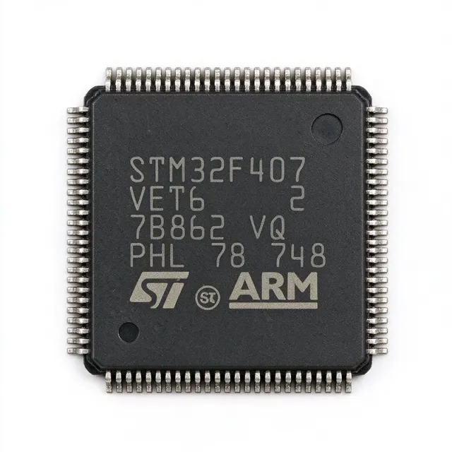
STM32F407VET6 - 168MHz Cortex-M4 MCU 512KB Flash LQFP-100 | ST
MPN: STM32F407VET6 ✓ Hoạt độngSTM32F407VET6 Tóm tắt
What is a microcontroller? A microcontroller (MCU) is a single-chip integrated circuit that combines a processor core, non-volatile program memory (Flash), volatile working memory (SRAM), and programmable peripherals to govern specific operations in embedded systems. The STM32F407VET6 belongs to the STM32F4 series built on the ARM Cortex-M4 core with FPU, positioned within the broader hierarchy of 32-bit MCUs - microcontroller in the embedded semiconductor taxonomy used in supply chains.
Key features include an on-chip 10/100 Ethernet MAC with IEEE 1588v2, USB 2.0 OTG Full-Speed and High-Speed with PHY, a digital camera interface (DCMI), three 12-bit ADCs with up to 24 channels and 2.4 MSPS, dual 12-bit DACs, an SDIO interface, FSMC for external memory, a crypto/hash peripheral, and a rich set of timers, USART, SPI, I2C, and CAN interfaces. The supply range is 1.8V to 3.6V with operation from -40C to +85C.
Technically, the STM32F407VET6 uses a Harvard bus architecture with separate instruction and data buses enabling simultaneous fetch and access, an ART Accelerator with 128-bit Flash prefetch eliminating wait states from Flash, a memory protection unit (MPU), and a nested vectored interrupt controller (NVIC) supporting deterministic real-time behavior. The single-precision FPU accelerates math-intensive firmware for control loops and DSP.
Typical applications include industrial motor control and PLCs, networked IoT gateways using the on-chip Ethernet MAC, USB device and host designs, and machine-vision or imaging systems using the DCMI camera interface.
Design tip: decouple every VDD pin with 100 nF ceramics plus bulk capacitance, route VDDA/VSSA on a clean analog plane to minimize ADC noise, and place the HSE crystal as close as possible with proper guard rings for stable clocking.
This page synthesizes distributor pricing, drop-in alternatives, and practical design considerations not found in the standalone manufacturer datasheet, including LQFP-100 same-footprint cross references and companion MPNs for reference designs.
Bộ thay thế dễ dàng lắp đặt cho STM32F407VET6 — cùng gói, chân-to-chân tương thích. Các bộ phận yêu cầu hàn PCB bị loại trừ.
Các biến thể trong loạt này
Các mẫu cùng loạt có thể lắp đặt dễ dàng tương thích với STM32F407VET6 (cùng hình factor và footprint) — khác nhau ở Package, SRAM, ADC, Communication Interfaces, Mounting Type.
STM32F407VGT6
Liên hệ để biết giá
Xem tài liệu →STM32F405VGT6
Liên hệ để biết giá
Xem tài liệu →STM32F427VIT6
Liên hệ để biết giá
Xem tài liệu →STM32F417VIT6
📋 Tham chiếu thay thế (không có trong danh mục)
GD32F407VET6
📋 Tham chiếu thay thế (không có trong danh mục)
GD32F407VGT6
📋 Tham chiếu thay thế (không có trong danh mục)
STM32F407VET6 Tỷ lệ tối đa & tính chất điện
| Core Architecture | ARM Cortex-M4F (32-bit RISC with FPU) |
| Tần số xung maksimum | 168 MHz |
| Program Memory (Flash) | 512 KB |
| SRAM | 192 KB |
| Hộp | LQFP-100 (14x14 mm) |
| Supply Voltage (VDD) | 1.8 V to 3.6 V |
| Nhiệt độ hoạt động | -40C to +85C |
| Bề rộng đường dữ liệu | 32 bit |
| ADC | 3 x 12-bit, up to 24 input channels |
| DAC | 2 x 12-bit |
| Communication Interfaces | USB OTG HS/FS, Ethernet MAC, 3x SPI, 3x I2C, 4x USART, 2x UART, 2x CAN, SDIO |
| Camera Interface | DCMI (Digital Camera Interface) |
| Kiểu lắp đặt | Surface Mount (SMD/SMT) |
| Cấp MSL | 3 (168 hours) |
| Trạng thái RoHS | Compliant |
| External Memory Bus | FSMC (Flexible Static Memory Controller) |
Cấu hình chân STM32F407VET6
| Chân 1 | PE2 — GPIO PE2 / TRACECLK / FSMC_A23 |
| Chân 2 | PE3 — GPIO PE3 / TRACED0 / FSMC_A19 |
| Chân 3 | PE4 — GPIO PE4 / TRACED1 / FSMC_A20 |
| Chân 4 | PE5 — GPIO PE5 / TRACED2 / FSMC_A21 |
| Chân 5 | PE6 — GPIO PE6 / TRACED3 / FSMC_A22 |
| Chân 6 | VBAT — Battery backup supply for RTC and backup registers |
| Chân 7 | PC13 — GPIO PC13 / RTC_TAMP1 / RTC_OUT / RTC_TS |
| Chân 8 | PC14 — GPIO PC14 / OSC32_IN |
| Chân 9 | PC15 — GPIO PC15 / OSC32_OUT |
| Chân 10 | VSS — Digital ground |
| Chân 11 | VDD — Digital supply (1.8V-3.6V) |
| Chân 12 | OSC_IN — HSE oscillator input |
| Chân 13 | OSC_OUT — HSE oscillator output |
| Chân 14 | NRST — Reset input (active low) |
| Chân 15 | PC0 — GPIO PC0 / ADC10_IN10 |
| Chân 16 | PC1 — GPIO PC1 / ADC11_IN11 |
| Chân 17 | PC2 — GPIO PC2 / ADC12_IN12 |
| Chân 18 | PC3 — GPIO PC3 / ADC13_IN13 |
| Chân 19 | VSSA — Analog ground |
| Chân 20 | VDDA — Analog supply (1.8V-3.6V) |
| Chân 21 | PA0/WKUP — GPIO PA0 / WKUP / ADC0_IN0 / TIM2_CH1 |
| Chân 22 | PA1 — GPIO PA1 / ADC1_IN1 / TIM2_CH2 |
| Chân 23 | PA2 — GPIO PA2 / ADC2_IN2 / TIM2_CH3 / USART2_TX |
| Chân 24 | PA3 — GPIO PA3 / ADC3_IN3 / TIM2_CH4 / USART2_RX |
| Chân 25 | VSS — Digital ground |
| Chân 26 | VDD — Digital supply |
| Chân 27 | PA4 — GPIO PA4 / ADC4_IN4 / DAC_OUT1 / SPI1_NSS |
| Chân 28 | PA5 — GPIO PA5 / ADC5_IN5 / DAC_OUT2 / SPI1_SCK |
| Chân 29 | PA6 — GPIO PA6 / ADC6_IN6 / SPI1_MISO / TIM13_CH1 |
| Chân 30 | PA7 — GPIO PA7 / ADC7_IN7 / SPI1_MOSI / TIM14_CH1 |
| Chân 31 | PC4 — GPIO PC4 / ADC14_IN14 |
| Chân 32 | PC5 — GPIO PC5 / ADC15_IN15 |
| Chân 33 | PB0 — GPIO PB0 / ADC8_IN8 / TIM3_CH3 |
| Chân 34 | PB1 — GPIO PB1 / ADC9_IN9 / TIM3_CH4 |
| Chân 35 | PB2 — GPIO PB2 / BOOT1 |
| Chân 36 | PE7 — GPIO PE7 / FSMC_D4 |
| Chân 37 | PE8 — GPIO PE8 / FSMC_D5 |
| Chân 38 | PE9 — GPIO PE9 / FSMC_D6 |
| Chân 39 | PE10 — GPIO PE10 / FSMC_D7 |
| Chân 40 | PE11 — GPIO PE11 / FSMC_D8 |
| Chân 41 | PE12 — GPIO PE12 / FSMC_D9 |
| Chân 42 | PE13 — GPIO PE13 / FSMC_D10 |
| Chân 43 | PE14 — GPIO PE14 / FSMC_D11 |
| Chân 44 | PE15 — GPIO PE15 / FSMC_D12 |
| Chân 45 | PB10 — GPIO PB10 / I2C2_SCL / USART3_TX |
| Chân 46 | PB11 — GPIO PB11 / I2C2_SDA / USART3_RX |
| Chân 47 | VSS — Digital ground |
| Chân 48 | VDD — Digital supply |
| Chân 49 | PB12 — GPIO PB12 / SPI2_NSS / I2C2_SMBA / USBOTGHS_ID |
| Chân 50 | PB13 — GPIO PB13 / SPI2_SCK / USBOTGHS_VBUS |
| Chân 51 | PB14 — GPIO PB14 / SPI2_MISO / USBOTGHS_DM |
| Chân 52 | PB15 — GPIO PB15 / SPI2_MOSI / USBOTGHS_DP |
| Chân 53 | PD8 — GPIO PD8 / FSMC_D13 / USART3_TX |
| Chân 54 | PD9 — GPIO PD9 / FSMC_D14 / USART3_RX |
| Chân 55 | PD10 — GPIO PD10 / FSMC_D15 |
| Chân 56 | PD11 — GPIO PD11 / FSMC_A16 |
| Chân 57 | PD12 — GPIO PD12 / FSMC_A17 |
| Chân 58 | PD13 — GPIO PD13 / FSMC_A18 |
| Chân 59 | PD14 — GPIO PD14 / FSMC_D0 |
| Chân 60 | PD15 — GPIO PD15 / FSMC_D1 |
| Chân 61 | PC6 — GPIO PC6 / I2S2_MCK / TIM8_CH1 / SDIO_D6 |
| Chân 62 | PC7 — GPIO PC7 / I2S3_MCK / TIM8_CH2 / SDIO_D7 |
| Chân 63 | PC8 — GPIO PC8 / TIM8_CH3 / SDIO_D0 |
| Chân 64 | PC9 — GPIO PC9 / I2C3_SDA / SDIO_D1 |
| Chân 65 | PA8 — GPIO PA8 / I2C3_SCL / USART1_CK / MCO1 |
| Chân 66 | PA9 — GPIO PA9 / USART1_TX / TIM1_CH2 / USBOTGFS_VBUS |
| Chân 67 | PA10 — GPIO PA10 / USART1_RX / TIM1_CH3 / USBOTGFS_ID |
| Chân 68 | PA11 — GPIO PA11 / USART1_CTS / USBOTGFS_DM |
| Chân 69 | PA12 — GPIO PA12 / USART1_RTS / USBOTGFS_DP |
| Chân 70 | PA13 — GPIO PA13 / JTMS-SWDIO |
| Chân 71 | VSS — Digital ground |
| Chân 72 | VDD — Digital supply |
| Chân 73 | PA14 — GPIO PA14 / JTCK-SWCLK |
| Chân 74 | PA15 — GPIO PA15 / JTDI / SPI3_NSS |
| Chân 75 | PC10 — GPIO PC10 / UART4_TX / SDIO_D2 |
| Chân 76 | PC11 — GPIO PC11 / UART4_RX / SDIO_D3 |
| Chân 77 | PC12 — GPIO PC12 / UART5_TX / SDIO_CK |
| Chân 78 | PD0 — GPIO PD0 / FSMC_D2 / CAN1_RX |
| Chân 79 | PD1 — GPIO PD1 / FSMC_D3 / CAN1_TX |
| Chân 80 | PD2 — GPIO PD2 / UART5_RX / SDIO_CMD |
| Chân 81 | PD3 — GPIO PD3 / FSMC_CLK |
| Chân 82 | PD4 — GPIO PD4 / FSMC_NOE |
| Chân 83 | PD5 — GPIO PD5 / FSMC_NWE |
| Chân 84 | PD6 — GPIO PD6 / FSMC_NWAIT |
| Chân 85 | PD7 — GPIO PD7 / FSMC_NCE2 / FSMC_NE1 |
| Chân 86 | PB3 — GPIO PB3 / JTDO / SPI3_SCK / I2S3_CK |
| Chân 87 | PB4 — GPIO PB4 / NJTRST / SPI3_MISO |
| Chân 88 | PB5 — GPIO PB5 / I2C1_SMBA / SPI3_MOSI / I2S3_SD |
| Chân 89 | PB6 — GPIO PB6 / I2C1_SCL / TIM4_CH1 / USART1_TX |
| Chân 90 | PB7 — GPIO PB7 / I2C1_SDA / TIM4_CH2 / USART1_RX |
| Chân 91 | BOOT0 — Boot mode selection (main Flash / system memory / SRAM) |
| Chân 92 | PB8 — GPIO PB8 / TIM4_CH3 / I2C1_SCL / CAN1_RX |
| Chân 93 | PB9 — GPIO PB9 / TIM4_CH4 / I2C1_SDA / CAN1_TX |
| Chân 94 | PE0 — GPIO PE0 / TIM4_ETR / FSMC_NBL0 |
| Chân 95 | PE1 — GPIO PE1 / FSMC_NBL1 |
| Chân 96 | VSS — Digital ground |
| Chân 97 | VSS — Digital ground |
| Chân 98 | VDD — Digital supply |
| Chân 99 | VDD — Digital supply |
| Chân 100 | VSS — Digital ground |
Ứng dụng tiêu biểu
STM32F407VET6 phù hợp cho 6 Áp dụngs: Industrial Motor Control and PLCs, Networked IoT Gateway with Ethernet, USB Device, Host and OTG Designs, Machine Vision and Imaging Systems, Audio Processing and DSP, Data Acquisition and Industrial Instrumentation.
Industrial Motor Control and PLCs
The STM32F407VET6 is well-suited for industrial motor control and PLC platforms where deterministic real-time performance is required. Its 168 MHz Cortex-M4F core with FPU and DSP extensions accelerates Park/Clarke transforms used in field-oriented control (FOC) for PMSM and ACIM motors. Three 12-bit ADCs at up to 2.4 MSPS enable simultaneous current and voltage sensing on all three motor phases for high-bandwidth torque control loops. Advanced timers with complementary PWM outputs and programmable dead-time insertion directly drive half-bridge power stages such as the STGIPN3H60 or gate drivers. Industrial operating temperature from -40C to +85C supports factory floor deployments, while CAN interfaces (2x) integrate with industrial fieldbus networks. Companion MPNs include STGIPN3H60 IGBT module, ACS712 current sensor, and isolated CAN transceiver.
Được đề xuất
Networked IoT Gateway with Ethernet
The STM32F407VET6 integrates a 10/100 Ethernet MAC with IEEE 1588v2 hardware timestamping that, paired with an external LAN8720A or DP83848 PHY, brings up a full TCP/IP gateway without an external Ethernet controller. Its 168 MHz Cortex-M4F core runs lwIP or similar stacks while reserving CPU headroom for application logic and TLS encryption accelerated by the on-chip crypto/hash peripheral. The 192 KB SRAM comfortably fits MQTT, CoAP, and TLS session buffers for typical edge gateway workloads, and the 512 KB Flash holds bootloader, application, and OTA staging partitions. USB OTG FS enables local configuration via mass storage or CDC, while SDIO supports local data logging. Companion MPNs include LAN8720A PHY, W25Q128JVSIQ NOR Flash for OTA, and TPS62135RGTR for power regulation.
Được đề xuất
USB Device, Host and OTG Designs
The STM32F407VET6 includes both USB OTG Full-Speed (12 Mbps) and High-Speed (480 Mbps) controllers with on-chip PHYs, enabling USB device, host, and OTG roles without external components. HS USB with the integrated ULPI-less PHY supports high-throughput functions such as mass storage, CDC ACM, HID, and audio class devices at full USB 2.0 speeds for industrial peripherals and test instruments. The 168 MHz Cortex-M4F core handles USB stack processing, class drivers, and application code concurrently, while 192 KB SRAM buffers USB packets efficiently. VBUS sensing pins and integrated 5V-tolerance on D+/D- simplify USB-C connector interfaces when paired with FUSB302 chipset. Companion MPNs include FUSB302UCX USB-C controller, USBLC6-2SC6 ESD protection, and TPS73633DBVR LDO.
Được đề xuất
Machine Vision and Imaging Systems
The STM32F407VET6 integrates a Digital Camera Interface (DCMI) that receives 8/10/12/14-bit parallel video streams from CMOS image sensors such as OV5640 or MT9V032, enabling cost-effective machine-vision and embedded imaging applications. The 168 MHz Cortex-M4F core runs JPEG/MJPEG compression, basic image processing, and feature extraction at video rates for applications like barcode scanning, optical inspection, and biometric capture. FSMC bus supports external SRAM or PSRAM buffering of full-resolution frames, while SDIO offloads captured images to SD cards at high speed. The camera interface synchronizes with on-chip timers for strobe/flash control. Companion MPNs include OV5640 image sensor, MT9V032 global shutter sensor, and IS42S16400F SDRAM for frame buffer.
Được đề xuất
Audio Processing and DSP
The STM32F407VET6 is well-suited for audio DSP applications thanks to its single-precision FPU and DSP instruction extensions on the Cortex-M4F core. Audio CODECs such as SGTL5000, WM8994, or CS43L22 interface to the MCU via I2S, providing stereo line/microphone inputs, headphone output, and integrated PLLs for low-jitter clocking. The 168 MHz core runs sample rates up to 192 kHz with headroom for EQ, mixing, and effects processing in real time on multiple audio channels. Dual 12-bit DACs provide analog audio output for simpler designs, and the SDIO interface reads audio files from SD cards for stand-alone players. Companion MPNs include SGTL5000 audio codec, CS43L22 DAC, and TPA6130A2 headphone amplifier.
Được đề xuất
Data Acquisition and Industrial Instrumentation
The STM32F407VET6 excels in multi-channel data acquisition systems where its three 12-bit ADCs (up to 24 channels, 2.4 MSPS total) capture analog signals simultaneously for power monitoring, condition monitoring, and instrumentation front-ends. The FPU and DSP extensions accelerate FFT-based frequency analysis for vibration, harmonic, and spectral measurements in industrial test equipment. FSMC interface supports external ADC converters (such as AD7606 16-bit) for higher resolution, while SDIO logs captured data to removable storage. The Ethernet MAC and USB OTG enable both bench-top SCPI-style instruments and networked remote data loggers. Industrial temperature rating of -40C to +85C supports factory floor installation. Companion MPNs include AD7606 16-bit ADC, AD620AN instrumentation amp, and TMP117 temperature sensor.
Được đề xuất
Tóm tắt các sản phẩm được đề xuất
Dữ liệu tham khảo kỹ thuật cho STM32F407VET6 — so sánh, hướng dẫn thiết kế và thông tin tuân thủ.
Hướng dẫn chọn lựa
So sánh với các sản phẩm thay thế
| Tham số | Sản phẩm này | STM32F407VGT6 | STM32F405VGT6 | STM32F417VIT6 | STM32F427VIT6 | GD32F407VET6 | GD32F407VGT6 |
|---|---|---|---|---|---|---|---|
| Package | LQFP-100 (14x14 mm) | LQFP-100 (14x14 mm) - same | LQFP-100 (14x14 mm) - same | LQFP-100 (14x14 mm) - same | LQFP-100 (14x14 mm) - same | LQFP-100 (14x14 mm) - same | LQFP-100 (14x14 mm) - same |
| Brand | STMicroelectronics | STMicroelectronics | STMicroelectronics | STMicroelectronics | STMicroelectronics | GigaDevice | GigaDevice |
| Core / Clock | Cortex-M4F / 168 MHz | Cortex-M4F / 168 MHz | Cortex-M4F / 168 MHz | Cortex-M4F / 168 MHz | Cortex-M4F / 180 MHz | Cortex-M4F / 168 MHz | Cortex-M4F / 168 MHz |
| Flash | 512 KB | 1 MB | 1 MB | 1 MB | 2 MB | 512 KB | 1 MB |
| SRAM | 192 KB | 192 KB | 192 KB | 192 KB | 256 KB | 192 KB | 192 KB |
| Ethernet MAC | Yes | Yes | No | Yes | Yes | Yes | Yes |
| USB OTG HS | Yes | Yes | Yes (no PHY) | Yes (with crypto) | Yes | Yes | Yes |
| Crypto / Hash | No | No | No | Yes (AES, Hash, RNG) | Yes | No | No |
| SDRAM Interface | No (FSMC only) | No (FSMC only) | No (FSMC only) | No (FSMC only) | Yes (SDRAM) | No (FSMC only) | No (FSMC only) |
| DCMI Camera IF | Yes | Yes | No | Yes | Yes | Yes | Yes |
| Approx. Unit Price | $5.95 (qty 1000) | $7.50 (qty 1000) | $6.20 (qty 1000) | $8.90 (qty 1000) | $9.40 (qty 1000) | $3.50 (qty 1000) | $4.30 (qty 1000) |
Bảo phân biệt quan trọng
- Pin-compatible upgrade path with more Flash (vsSTM32F407VGT6)
- More memory than STM32F407VET6 in same LQFP-100 (vsSTM32F427VIT6)
- Cryptographic acceleration absent on STM32F407VET6 (vsSTM32F417VIT6)
- Cost-effective cross-brand second source (vsGD32F407VET6)
Ghi chú thiết kế
Decouple every VDD pin with a 100 nF X7R ceramic placed within 2 mm of the pin, plus a shared 4.7 uF bulk capacitor on each supply rail. The VDDA analog supply should be filtered with a ferrite bead from VDD and bypassed with 10 nF + 1 uF ceramics to minimize ADC noise. If VREF+ is used, drive it from a low-noise reference source; otherwise tie it to VDDA and accept the reduced ADC linearity. Refer to ST application note AN5031 for STM32F4 power-supply hardware design guidelines.
Place the 8 MHz HSE crystal within 5 mm of OSC_IN/OSC_OUT with symmetric traces and a ground guard ring. Route the 32.768 kHz LSE crystal traces short and away from switching nodes, with the load capacitors placed adjacent. Use a 4-layer PCB with continuous ground plane beneath the MCU; for LQFP-100, fan out signals on inner layers to maintain a low-impedance ground return path under the package. ESD protection (TVS arrays) should be placed near any external connector pins.
The STM32F407VET6 in LQFP-100 has a typical junction-to-ambient thermal resistance (theta_JA) of approximately 50 C/W depending on PCB copper area. For applications where the MCU runs near full 168 MHz with all peripherals active, design the ground copper pour under the package to at least 1 square inch to keep junction temperature below 100 C. The internal temperature sensor can be read by application firmware for thermal monitoring and dynamic clock throttling. Refer to ST datasheet DM00037051 for thermal characteristics.
Avoid leaving unused GPIO pins in floating input state; configure them as analog inputs to minimize current leakage. The BOOT0 pin must be held low for normal Flash boot; if left floating, the bootloader may enter system memory and stall. When using the integrated Ethernet MAC, ensure the external PHY is brought up before RMII/MII clock is enabled, or the MCU may hang during PHY initialization. Verify HSE crystal load capacitance matches the crystal specification - typical 8 MHz crystals need 10-20 pF load.
The high-speed USB OTG HS DP/DM traces must be 90 ohm differential impedance matched, length-matched within 150 mil, and routed over a continuous ground plane with no splits. For Ethernet RMII traces between MCU and external PHY, length-match the clock and data lines and keep traces under 50 mm. SDIO and FSMC bus signals should be length-matched within 1 inch when running at the maximum clock rate; place series damping resistors near the driver to control ringing.
Thông tin tuân thủ
RoHS and REACH compliant per STMicroelectronics product page DM00037051. Not AEC-Q100 qualified; for automotive grade, consider STM32F407VET7 or STM32F407VET6 automotive screening options. Lead-free and halogen-free per ST product certification.