IRF7380TRPBF vs IRF7854TRPBF 比較
詳細並排比較 IRF7380TRPBF 由 Infineon 與 IRF7854TRPBF 由 Infineon. 比較關鍵規格、電氣參數、封裝、生命週期狀態、價格與供貨情況,以找出最符合您設計需求的元件。

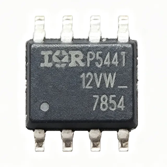
規格比較
| 參數 | IRF7380TRPBF | IRF7854TRPBF |
|---|---|---|
| 品牌 | Infineon | Infineon |
| 類別 | MOSFETs | MOSFETs |
| 生命週期狀態 | 啟用中 | 啟用中 |
| 單價 (USD) | — | $0.48 |
| Manufacturer | Infineon Technologies (formerly International Rectifier) | — |
| Part Number | IRF7380TRPBF | — |
| Configuration | Dual N-Channel MOSFET Array (2 independent FETs in one package) | — |
| Drain-to-Source Voltage (VDS) | 80 V | — |
| Continuous Drain Current (ID) | 3.6 A | — |
| On-Resistance RDS(on) max | 73 mOhm at VGS = 10 V | — |
| Technology | IR MOSFET™ (Infineon HEXFET-style planar N-ch) | HEXFET (planar N-channel) |
| Total Power Dissipation (PD) | 2 W | — |
| 封裝 | SO-8 (8-SO, SOIC-8) | SO-8 |
| 安裝類型 | Surface Mount | Surface Mount |
| 工作接面溫度 | -55 C to +150 C | — |
| Gate Drive Voltage (typical) | 10 V (full RDS(on)); logic-level not guaranteed | — |
| Lead-Free / RoHS | Yes (Pb-free plating, suffix PBF) | Yes (PBF suffix, lead-free) |
| Packaging | Tape & Reel (suffix TR) | — |
| Primary Application | High-frequency DC-DC converters | — |
| FET Type | — | N-Channel |
| Drain-Source Voltage (VDS) | — | 80 V |
| Continuous Drain Current (ID) at Ta=25°C | — | 10 A |
| Power Dissipation (PD) at Ta=25°C | — | 2.5 W |
| On-Resistance RDS(on) max at VGS=10V | — | 13.4 mΩ |
| Gate-Source Threshold Voltage VGS(th) max | — | 4.9 V |
| Total Gate Charge Qg | — | 27 nC |
| 工作溫度範圍 | — | -55°C to +150°C (TJ) |
| Qualification | — | JEDEC industrial, Normal level |
| Solder Process | — | Reflow and wave-solderable |
| Gate Drive Voltage (recommended) | — | 10 V |