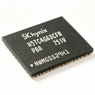
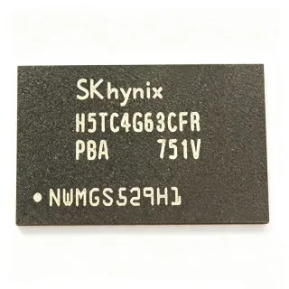
H5ANAG6NCR-UHC - 16Gb DDR4 SDRAM 1Gx16 FBGA-96 | SK Hynix
MPN: H5ANAG6NCR-UHC ✓ 啟用中H5ANAG6NCR-UHC 概覽
DDR4 SDRAM (Double Data Rate fourth-generation synchronous DRAM) is the dominant volatile main-memory technology for servers, desktops, industrial controllers, and embedded computing modules. Within the memory hierarchy, a DDR4 SDRAM sits below the CPU cache and above storage, providing random access to working data at multi-gigabit-per-second transfer rates while requiring a memory controller to manage refresh, bank activation, and command timing.
Key characteristics of this family include a 16Gbit monolithic die density, a x16 data interface that simplifies 16-bit and 32-bit memory bus designs, and DDR4 features such as bank groups, burst length 8, and on-die termination. The UHC speed suffix denotes a commercial/industrial operating-range speed grade within the H5ANAG6N family, and the C die revision is a later-generation shrink of the A-die H5ANAG6NAMR, typically offering improved power characteristics.
Architecturally, the device organizes capacity into multiple banks and bank groups addressed by row and column strobes, using a 1.2V-class core supply typical of DDR4. Internal pipelining and DLL-based clocking sustain high-burst bandwidth, while DDR4 protocol features reduce command bus contention versus DDR3.
Typical applications include main memory for embedded x86 and ARM computing modules, industrial controllers requiring large working memory, network appliances, data logging systems, and replacement sourcing for aging DDR4 BOMs. The x16 organization suits cost-optimized boards where a full 64-bit bus is not required.
Designers should verify controller compatibility with the die revision C timing set, implement DDR4 fly-by routing with proper termination, and confirm the exact speed grade suffix against the ordering information table in the official datasheet.
This page synthesizes distributor availability data, same-family drop-in variants, and practical DDR4 design guidance not consolidated in the manufacturer datasheet, with all unverified parameters explicitly flagged for engineering review.
直接替換替代品,適用於 H5ANAG6NCR-UHC — 相同封裝,腳位對腳位相容。需重新設計 PCB 的不同封裝零件不列入。
此系列的變體
與下列產品可直接替換的同系列型號: H5ANAG6NCR-UHC (相同外形與佔位) — 差異在於 Package, Interface, Organization, Density, Mounting Type.
H5ANAG6NAMR-UHC
✅ 直接替換聯絡詢價
查看資料表 →H5ANAG6NCR-RDC
✅ 直接替換聯絡詢價
查看資料表 →H5ANAG6NCR-PBC
✅ 直接替換聯絡詢價
查看資料表 →H5ANAG6NCJR-XNC
✅ 直接替換 ⚠️ 規格未經驗證✓ 有庫存
$68.9063 / 單位
查看資料表 →H5ANAG6NBJR-UHC
✅ 直接替換 ⚠️ 規格未經驗證聯絡詢價
查看資料表 →H5ANAG8NCR-UHC
✅ 直接替換 ⚠️ 規格未經驗證聯絡詢價
查看資料表 →H5ANAG6NCR-UHC 規格
| 記憶體類型 | DDR4 SDRAM |
| Memory Density | 16 Gb (2 GB) |
| 組織 | 1G x 16 |
| 介面 | CMOS, Double Data Rate IV |
| 封裝 | FBGA-96 (PBGA-96) |
| Die Revision | C |
| Configuration | 1 Channel, 1 Rank |
| 安裝類型 | Surface Mount |
| Application | Main memory, embedded computing, industrial controllers |
H5ANAG6NCR-UHC fbga-96 (pbga-96) 腳位配置指南
H5ANAG6NCR-UHC(fbga-96 (pbga-96) 封裝)的腳位配置。 腳位編號、功能與連接圖定義於製造商資料手冊中。請參閱該手冊以取得確切的封裝尺寸與焊接指引。

無詳細腳位定義資料: H5ANAG6NCR-UHC.
請參閱 資料表 以查看完整腳位配置。
典型應用
H5ANAG6NCR-UHC 適用於 6 應用s: Embedded Computing Modules, Industrial Controllers, Network Appliances, Data Logging and Embedded Storage Caching, Test and Measurement Instruments, Replacement Sourcing and BOM Continuity.
Embedded Computing Modules
Embedded x86 and ARM computing modules (COM Express, SMARC, custom SoMs) need dense main memory in minimal board area. The H5ANAG6NCR-UHC provides 2GB per package at 1Gx16 organization in a 0.8 x 1.0-inch-class 96-ball FBGA, so a module can reach 4GB with just two components on a 32-bit bus. The x16 strobe configuration (UDQS/LDQS) simplifies length-matched routing versus eight x8 parts. Because DDR4 uses a fly-by clock topology with on-die termination, the memory controller's ZQ calibration and write-leveling must be run at bring-up; expect to reserve VTT termination rail budget of roughly half the VDDQ current for a 1.2V-class DDR4 interface.
推薦
Industrial Controllers
Industrial PLCs and motion controllers increasingly run Linux-class firmware that demands gigabytes of working memory for protocol stacks, logging buffers, and HMI rendering. The H5ANAG6NCR-UHC supplies 16Gb density in one FBGA-96 component, reducing BOM line count versus stacking 4Gb parts, and its x16 bus suits the 16/32-bit controllers common in industrial designs. Layout should follow the SK hynix DDR4 design guide: fly-by address/command routing, 40-ohm-class series termination at the controller, and solid VDDQ plane segmentation. Industrial enclosures with limited airflow require derating analysis of the component's operating-temperature specification before qualification.
推薦
Network Appliances
Packet-processing appliances, security gateways, and router line cards use DDR4 for flow tables, packet buffers, and deep-packet-inspection state. The H5ANAG6NCR-UHC's 1Gx16 organization allows granular memory sizing on 32-bit sub-channels, and 16Gb per package maximizes state capacity per PCB area, directly increasing supported concurrent sessions. Designers should pair the DRAM with a dedicated memory controller or network processor supporting DDR4 burst length 8 and bank-group interleaving, since bank-group scheduling measurably raises effective bandwidth for random-access-heavy packet workloads. Confirm refresh (tRFC) overhead in latency budgets when sizing buffer depth.
推薦
Data Logging and Embedded Storage Caching
Embedded loggers, gateways, and test instruments use DDR4 as a write cache between high-speed acquisition front ends and slower NAND storage. The H5ANAG6NCR-UHC offers 2GB of buffering in one component; at a 100 MB/s sustained ingest rate this buffer represents roughly 20 seconds of data, enough to absorb NAND erase-cycle stalls without loss. The x16 organization reduces strobe count and simplifies the layout on two-layer-stack instrumentation boards. Designers must implement controller-side wear-aware flushing and power-fail handling, since DDR4 is volatile - pair the DRAM with a supervisor that triggers a safe flush or a backup-energy dump on brownout detection.
推薦
Test and Measurement Instruments
Oscilloscopes, logic analyzers, and signal generators require deep acquisition memory to capture long time records at high sample rates. The H5ANAG6NCR-UHC, at 16Gb per component, lets an instrument implement multi-gigabyte capture buffers using four packages on a 64-bit bus. DDR4's burst architecture favors the sequential-write pattern of acquisition streaming, and bank-group interleaving sustains near-peak bandwidth for continuous recording. Thermal design matters in benchtop instruments: DDR4 components at sustained streaming loads dissipate measurable power, so placement near fans and copper pour under the FBGA-96 thermal balls improves junction-to-ambient conditions during long captures.
推薦
Replacement Sourcing and BOM Continuity
Many legacy DDR4-based platforms face obsolescence of older die revisions, forcing replacement sourcing. The H5ANAG6NCR-UHC (C die) is a natural substitute for designs qualified around earlier family members such as the H5ANAG6NAMR (A die) or H5ANAG6NBJR, because all share the same 96-ball FBGA footprint, 1Gx16 organization, and DDR4 protocol interface - no PCB rework is required. The recommended procedure is: confirm the controller timing table against die-revision C data, run a full memory stress test (e.g., extended margin scanning), and update the AVL. This keeps production lines running while capturing the shrink-die benefits of reduced operating current.
推薦
推薦產品摘要
工程參考資料,適用於 H5ANAG6NCR-UHC — 比較、設計指引及合規資訊。
選型指南
與替代品比較
| 參數 | 本產品 | H5ANAG6NAMR-UHC | H5ANAG6NCR-RDC | H5ANAG6NCR-PBC | H5ANAG6NCJR-XNC | H5ANAG6NBJR-UHC | H5ANAG8NCR-UHC |
|---|---|---|---|---|---|---|---|
| Package | FBGA-96 | FBGA-96 - same | FBGA-96 - same | FBGA-96 - same | FBGA-96 - same | FBGA-96 - same | FBGA-96 - same |
| Brand | SK Hynix | SK Hynix | SK Hynix | SK Hynix | SK Hynix | SK Hynix | SK Hynix |
| Density | 16 Gb (2 GB) | 16 Gb | 16 Gb | 16 Gb | 16 Gb | 16 Gb | 16 Gb |
| Organization | 1G x 16 | 1G x 16 | 1G x 16 | 1G x 16 | 1G x 16 | 1G x 16 | 2G x 8 |
| Memory Type | DDR4 SDRAM | DDR4 SDRAM (DDR4-2400 class family) | DDR4 SDRAM | DDR4 SDRAM | DDR4 SDRAM | DDR4 SDRAM | DDR4 SDRAM |
| Die Revision | C | A | C | C | J | B | C |
| Speed Grade Suffix | UHC | UHC - same | RDC - different bin | PBC - different bin | XNC - different bin | UHC - same | UHC - same |
主要差異化特點
- Newest C die revision in the 16Gb family (對比H5ANAG6NAMR-UHC)
- Identical UHC speed grade as legacy sibling (對比H5ANAG6NBJR-UHC)
- x16 organization reduces bus complexity (對比H5ANAG8NCR-UHC)
設計說明
DDR4 requires fly-by routing of address/command/clock with on-die termination and controller-side write leveling. For the x16 H5ANAG6NCR-UHC, keep UDQS/UDQS# and LDQS/LDQS# diff pairs length-matched within +/-5 mils internally and match DQ to its strobe within the controller's specified skew window (typically a few hundred picoseconds). Route at 40-50 ohm single-ended impedance, reference DQ routing to a continuous VDDQ plane, and avoid crossing plane splits under the FBGA-96 fanout. Follow the SK hynix DDR4 design guide for series-termination placement at the controller end.
DDR4 uses separate VDD (core) and VDDQ (interface) rails, nominally 1.2V-class per JEDEC DDR4 convention - confirm exact ranges in the die-revision C datasheet. Estimated: a 16Gb x16 DDR4 operating at DDR4-2400-class rates draws peak currents in the hundreds of milliamps per component; size the VTT termination regulator for roughly half of total VDDQ current and place bulk (100 uF class) plus high-frequency (0.1 uF) decoupling at each rail pin group. VPP, if specified for the family, is a separate 2.5V-class rail - never share it with VDD.
Do not assume datasheet interchange between die revisions. The A-die H5ANAG6NAMR datasheet is the most widely mirrored document, but the C-die H5ANAG6NCR may have updated timing (tRFC, tFAW) and IDD tables; controllers programmed with stale timing sets can show marginal reliability at temperature extremes. Always pull the die-revision-C document from SK hynix before programming controller registers, and re-run write-leveling and read-eye training after any die-revision or speed-suffix change in production.
合規資訊
Verified web data contains no explicit RoHS/REACH certificate for this exact suffix. Modern SK hynix DDR4 is typically produced as green (lead-free/halogen-free) packaging, but official certificates must be obtained from SK hynix or the distributor. Not an automotive-qualified ordering code.