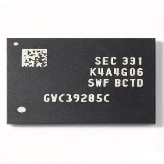
H5ANAG6NAMR-UHC - 16Gb DDR4-2400 SDRAM x16 1.2V | SK hynix
MPN: H5ANAG6NAMR-UHC ✓ Active| Qty | Unit Price | Extended |
|---|---|---|
| 1 | $6.2 | $6.20 |
| 10 | $5.75 | $57.50 |
| 100 | $5.2 | $520.00 |
| 500 | $4.85 | $2,425.00 |
| 1,000 | $4.5 | $4,500.00 |
H5ANAG6NAMR-UHC Overview
DDR4 SDRAM is the fourth generation of Double Data Rate synchronous dynamic random access memory, a type of volatile memory that stores data in capacitor-based cells refreshed at regular intervals. Within the memory hierarchy, DDR4 sits below LPDDR (mobile) and above DDR3, offering higher density, lower operating voltage, and bank-group architecture. It is the dominant DRAM class for computing modules, industrial controllers, and networking equipment main memory.
Key features of this component include 16Gb density organized as 1G x 16, a low 1.2V core supply that reduces power consumption versus DDR3 (1.5V), and the bank-group architecture of DDR4 that enables higher effective bandwidth at moderate clock rates. The x16 organization simplifies bus design for embedded controllers that cannot implement full 64-bit DDR4 channels. The CMOS process die supports normal power class operation.
Technically, the H5ANAG6NAMR family is a 16Gb CMOS Double Data Rate IV SDRAM suited for main memory applications requiring large density and bandwidth, according to the SK hynix Consumer DDR4 H5ANAG6NAMR datasheet (Rev1.0). The die supports multiple speed bins (PB/RD/TF/UH/VK), with UHC corresponding to DDR4-2400 timing. The FBGA package minimizes board area and improves signal integrity versus older TSOP packaging.
Typical applications include industrial controller main memory, firmware boot and embedded logging buffers, computing modules (SODIMM/COM Express), networking equipment line-card memory, and replacement sourcing for legacy DDR4 BOM lines.
Design consideration: x16 DDR4 devices use differential data strobes and a dedicated reset pin; ensure the controller supports 16-bit DDR4 mapping and that VDDQ termination follows the SK hynix reference design for 2400 MT/s signal integrity.
This page synthesizes distributor availability data, same-package alternatives, and drop-in substitution guidance not consolidated in the manufacturer datasheet.
Drop-in alternatives for H5ANAG6NAMR-UHC — same package, pin-to-pin compatible. Different-package parts requiring PCB rework are excluded.
Variants in this series
Same-series models that are drop-in compatible with H5ANAG6NAMR-UHC (same form factor and footprint) — differing in Interface, Package, Data Rate, Organization, Memory Density.
Quick Comparison Tool — Select alternative parts for side-by-side comparison:
H5ANAG6NBJR-UHC
✅ Drop-In✓ In Stock
$8.09 / Unit
View Datasheet →H5ANAG6NBJR-VKC
✅ Drop-In✓ In Stock
$15 / Unit
View Datasheet →H5ANAG6NCJR-XNC
✅ Drop-In✓ In Stock
$84.97 / Unit
View Datasheet →H5ANAG8NAMR-UHC
✅ Drop-In✓ In Stock
$2.15 / Unit
View Datasheet →H5ANAG8NCMR-VKC
✅ Drop-In✓ In Stock
$8.05 / Unit
View Datasheet →H5ANAG6NAMR-UHC Maximum Ratings & Electrical Characteristics
| Memory Type | DDR4 SDRAM |
| Memory Density | 16 Gbit (2 GB) |
| Organization | 1G x 16 |
| Speed Grade / Data Rate | DDR4-2400 (UHC bin, PC4-19200) |
| Supply Voltage (VDD) | 1.2 V |
| Architecture | CMOS DDR4 with bank groups |
| Power Class | Normal Power |
| Package | FBGA-96 (PBGA96) |
| Mounting Type | Surface Mount (BGA solder ball) |
| Refresh | Self-refresh and auto-refresh (DDR4 standard 64 ms) |
| Interface Type | Parallel, synchronous, double data rate |
| Available Speed Bins (family) | PB / RD / TF / UH / VK |
| Application Class | Main memory, embedded, industrial |
| Lifecycle Status | Active production |
H5ANAG6NAMR-UHC fbga-96 (pbga96) Pin Configuration Guide
Pin configuration for H5ANAG6NAMR-UHC (fbga-96 (pbga96) package). This digital IC includes GPIO, communication interfaces (UART, SPI, I2C), and power pins. Refer to the manufacturer datasheet for alternate pin functions and configuration options. Essential for embedded system design and PCB layout.

No detailed pinout data available for H5ANAG6NAMR-UHC.
Refer to the datasheet for full pin configuration.
Typical Applications
H5ANAG6NAMR-UHC is suitable for 6 applications: Industrial Controller Main Memory, Firmware Boot and Embedded Logging, Computing Modules (SODIMM / COM Express), Networking Equipment Line Cards, Test and Measurement Instrumentation, DDR4 Replacement Sourcing / BOM Maintenance.
Industrial Controller Main Memory
Industrial controllers and PLCs benefit from the H5ANAG6NAMR-UHC's 16Gb (2 GB) density in a single x16 chip, which reduces component count versus four 4Gb parts while keeping the memory bus width manageable at 16 bits. The 1.2V DDR4 supply cuts DRAM power roughly in half versus comparable DDR3 solutions, lowering heat load inside sealed industrial enclosures. Placed on a 16-bit DDR4 channel at DDR4-2400, the chip delivers sufficient bandwidth for deterministic control loops, recipe storage caching, and HMI buffering. Its normal power class and self-refresh support allow the controller to suspend into low-power states between scan cycles, extending life in battery-backed and energy-harvesting installations.
Recommended
Firmware Boot and Embedded Logging
The H5ANAG6NAMR-UHC serves as working memory for firmware boot loaders and high-rate embedded logging systems where flash write bandwidth is insufficient for temporary buffering. The 16Gb x16 organization allows log data to be captured into DRAM at DDR4-2400 burst rates and flushed to flash in efficient sequential writes, protecting wear-leveling budgets on NOR/NAND boot devices. Differential data strobes maintain timing margin across industrial temperature swings, and the DDR4 reset pin guarantees a defined memory state after brown-out events - critical for logging integrity. Designers typically pair it with an EEPROM or serial flash boot device and configure the memory controller for 2 GB per-rank addressing.
Recommended
Computing Modules (SODIMM / COM Express)
On computing modules such as COM Express and SMARC carriers, the H5ANAG6NAMR-UHC provides 2 GB per soldered-down chip, enabling onboard (non-socketed) memory designs that survive vibration better than SODIMM sockets. Two x16 chips create a 32-bit channel at DDR4-2400, delivering multi-GB/s bandwidth for embedded x86 and ARM processors. The FBGA-96 package's short ball interconnects improve signal integrity at 1200 MHz clocks compared with socketed DIMMs, allowing shorter trace lengths and relaxed layout constraints. Designers should follow the module's memory controller drive-strength and ODT (on-die termination) configuration from the SK hynix datasheet for stable operation.
Recommended
Networking Equipment Line Cards
Network line cards and switch management CPUs use the H5ANAG6NAMR-UHC for packet buffer and control-plane memory. The DDR4 bank-group architecture provides the interleaved access pattern that packet-buffer engines need, while 16Gb per chip allows large buffering depth (multi-GB) without populating full 64-bit ranks. The 1.2V VDDQ domain keeps power per Gbps of buffering low, which matters in fanless access equipment. At DDR4-2400 in a 16-bit configuration, a pair of chips sustains the burst traffic of Gigabit-class switching. Controller configurations should enable per-bank refresh scheduling to bound latency spikes during refresh windows.
Recommended
Test and Measurement Instrumentation
Oscilloscope and logic analyzer front ends require deep capture memory with sustained write bandwidth; the H5ANAG6NAMR-UHC's DDR4-2400 interface and 2 GB capacity per chip make it suitable for acquisition buffer stages in mid-range instruments. The x16 organization simplifies interleaving multiple chips across a wide acquisition bus, and DDR4's burst architecture matches the streaming nature of ADC sample capture. Because instrument vendors value multi-sourcing, the SK hynix family's die revisions (AMR/BJR/CJR) and the Micron equivalent provide drop-in second sources within the same FBGA-96 layout, reducing BOM risk in long-lifetime T&M platforms.
Recommended
DDR4 Replacement Sourcing / BOM Maintenance
For BOM maintenance on legacy DDR4 platforms, the H5ANAG6NAMR-UHC is a frequently requested replacement line: distributor catalogs (Datasheet Directory, Censtry, IC-Components) position it explicitly for replacement sourcing. Because the H5ANA family shares the FBGA-96 x16 footprint across density and speed variants, buyers can substitute H5ANAG6NBJR-UHC or H5ANAG6NCJR-XNC during shortages with layout unchanged, then re-validate timing in the memory controller. Procurement teams should hold a qualified second source and verify date codes, since DDR4 broker stock varies in manufacturing vintage; all substitutions should be re-run through the platform's memory training procedure before release.
Recommended
Recommended Products Summary
Engineering reference data for H5ANAG6NAMR-UHC — comparison, design guidance, and compliance information.
Selection Guide
Comparison with Alternatives
| Parameter | This Product | H5ANAG6NBJR-UHC | H5ANAG6NBJR-VKC | H5ANAG6NCJR-XNC | H5ANAG8NAMR-UHC | H5ANAG8NCMR-VKC |
|---|---|---|---|---|---|---|
| Package | FBGA-96 (PBGA96) | FBGA-96 - same | FBGA-96 - same | FBGA-96 - same | FBGA-96 - same | FBGA-96 - same |
| Brand | SK Hynix | SK Hynix | SK Hynix | SK Hynix | SK Hynix | SK Hynix |
| Density | 16 Gbit (2 GB) | 16 Gbit | 16 Gbit | 16 Gbit | 8 Gbit (1 GB) | 8 Gbit (1 GB) |
| Organization | 1G x 16 | 1G x 16 | 1G x 16 | 1G x 16 | 512M x 16 | 512M x 16 |
| Supply Voltage | 1.2 V | 1.2 V | 1.2 V | 1.2 V | 1.2 V | 1.2 V |
| Die Revision | AMR | BJR | BJR | CJR | AMR | CMR |
Key Differentiators
- Double the density per chip versus 8Gb alternatives (vs H5ANAG8NAMR-UHC)
- Balanced speed bin for industrial designs (vs H5ANAG6NBJR-VKC)
- x16 organization simplifies narrow-channel designs (vs MT40A1G16TD-062E (functionally identical) and x8-based DDR4 parts generally)
Design Notes
Route the DDR4-2400 x16 bus with length-matched DQ/DQS/DM groups and control/address fly-by topology per the SK hynix datasheet layout guidelines. Keep DQS differential pairs tightly coupled (gap less than 2x trace width) and match intra-pair skew to under 5 mils. Because the FBGA-96 ball map uses separate VDD and VDDQ ball groups, allocate independent power planes with bulk (47-100 uF) and per-ball (0.1 uF) decoupling; DDR4 at 1200 MHz clock is sensitive to rail noise on VPP and VDDQ.
The 1.2V rail powers both core and I/O domains. Estimated IDD at DDR4-2400 for a 16Gb x16 die is on the order of hundreds of milliamps per device in active read/write bursts - budget the PMIC DDR4 rail for at least 0.5 A per chip plus termination current. Verify VPP (2.5V) presence, since DDR4 requires it for cell word-line drive; omitting VPP decoupling is a common cause of marginal training results.
Do not assume all H5ANA family variants share identical timing registers: CJR and BJR die revisions can require different MR (mode register) drive-strength and ODT settings than the AMR die in this part. Always re-run memory training after any BOM substitution and update SPD/controller configuration tables. Cross-brand substitutions (e.g., Micron x16 FBGA) are footprint-compatible in principle but must be validated at the board level for drive strength and refresh behavior before production.
Compliance Information
Compliance declarations were not present in the provided verified web data. Request SK hynix RoHS/REACH declarations from the manufacturer product page or distributor before final qualification.