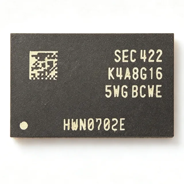
K4A8G165WG-BCWE - 8Gb DDR4 SDRAM 3200Mbps 1.2V | Samsung
部品番号: K4A8G165WG-BCWE ✓ 生産中| 数量 | 単価 | 小計 |
|---|---|---|
| 1 | $44.97 | $44.97 |
| 10 | $42.72 | $427.20 |
| 100 | $40.47 | $4,047.00 |
| 500 | $38.22 | $19,110.00 |
| 1,000 | $35.98 | $35,980.00 |
K4A8G165WG-BCWE 概要
DDR4 SDRAM (Double Data Rate 4 Synchronous Dynamic Random Access Memory) is the fourth generation of the JEDEC DDR DRAM family. A DRAM stores each bit in a capacitor-based memory cell that must be periodically refreshed, and the synchronous interface means all operations are timed to a clock signal. Within the memory hierarchy, the K4A8G165WG-BCWE sits at the main-memory component level: DRAM cell -> DDR4 SDRAM -> synchronous DRAM -> volatile memory IC -> semiconductor. Compared with DDR3, DDR4 lowers the core supply from 1.5V to 1.2V, raises bank-group parallelism, and improves burst length and prefetch efficiency, so system designers gain both bandwidth and power savings.
Key features include the 8 Gbit density in a single x16-wide device, a 3200 Mbps/pin maximum data rate (PC4-25600 class), and the 1.2V operating supply that reduces dynamic power versus 1.35V DDR3L alternatives. The commercial temperature range of 0C to +85C suits desktop, consumer, and networking equipment but not extended-temperature industrial designs (the -I grade variant serves that need). Samsung B-die based construction is well regarded for tight timing margins.
Architecturally, the device uses a 16n prefetch with bank groups, enabling high effective bandwidth while keeping internal core speeds manageable. On-die termination, DLL, and ZQ calibration circuits maintain signal integrity across the high-speed command/address and data buses as defined by the DDR4 SDRAM standard.
Typical applications include desktop PC and workstation DIMMs, embedded CPU memory subsystems (ARM/x86 SoCs), networking routers and switches, industrial gateways, and consumer electronics requiring 1-8 GB of main memory per board.
Design consideration: DDR4 fly-by routing requires per-DRAM write leveling and careful length matching; budget ~1.2V +/- 3% (per Samsung datasheet) and verify termination against your memory controller's supported speed grade.
This page synthesizes distributor pricing, stock data, drop-in alternatives, and practical design notes not found in the Samsung datasheet alone.
ドロップイン代替品: K4A8G165WG-BCWE — 同一パッケージでピン互換。PCBの作り直しが必要な異なるパッケージの部品は除外されています。
クイック比較ツール — 並列比較する代替部品を選択:
K4A8G165WC-BCWE
✓ 在庫あり
$38 / 個
データシートを見る →K4A8G165WB-BCWE
✓ 在庫あり
$6.55 / 個
データシートを見る →H5AN8G6NDJR-UHC
✓ 在庫あり
$34.6 / 個
データシートを見る →NT6AN8T6WBJ1B1
✓ 在庫あり
$8.75 / 個
データシートを見る →MT40A512M16LY-062E IT:E
📋 参考代替品(カタログ未掲載)
K4A8G165WG-BCWE 最大定格&電気的特性
| メモリタイプ | DDR4 SDRAM (Volatile DRAM) |
| メモリサイズ | 8 Gbit |
| Memory Organization | 512M x 16 |
| インターフェース | Parallel |
| Max Data Rate | 3200 Mbps/pin |
| Clock Cycle Time | 19 ns |
| 電源電圧 | 1.2 V |
| パッケージ | FBGA-96 (BGA-96), surface mount |
| 動作温度 | 0C to +85C (commercial) |
| Refresh | Auto/self refresh per DDR4 standard |
| 実装タイプ | Surface Mount |
| RoHS ステータス | Compliant |
| Manufacturer | Samsung Semiconductor, Inc. |
| Product Status | Active |
| Typical Standby Current | 20 mA (per LCSC listing) |
| Die Generation | Samsung B-die, 8Gb DDR4 x16 |
K4A8G165WG-BCWE fbga-96 (bga-96), surface mount ピン配置ガイド
K4A8G165WG-BCWE (fbga-96 (bga-96), surface mount パッケージ) のピン配置。 このデジタルICには、GPIO、通信インターフェース (UART、SPI、I2C)、および電源ピンが含まれています。代替ピン機能と設定オプションについては、メーカーのデータシートを参照してください。組み込みシステム設計とPCBレイアウトに不可欠です。

詳細なピン配置データはありません: K4A8G165WG-BCWE.
詳細は データシート をご参照ください。
主な用途
K4A8G165WG-BCWE の用途: 6 件s: Desktop PC and Workstation DIMM Main Memory, Embedded SoC Memory Subsystem, Networking Routers and Switches, Industrial Gateways and Edge Computing, Consumer Electronics and Smart TV, Test, Measurement, and FPGA Memory Expansion.
Desktop PC and Workstation DIMM Main Memory
The K4A8G165WG-BCWE's 8Gb density and 3200 Mbps data rate make it a mainstream building block for desktop DDR4 UDIMMs at the PC4-25600 speed class. Soldered eight or sixteen x16 devices per module, a single-rank 8 GB DIMM uses eight of these chips across the 64-bit data bus, delivering 25.6 GB/s peak bandwidth at 1.2V. The x16 organization halves the chip count versus x8 parts for a given bus width, reducing BOM cost on consumer modules. Because the device is commercial-temperature (0C to +85C) rated, it fits typical office and home desktop thermal envelopes where case airflow keeps DIMM surfaces below 85C. Per the Samsung datasheet, standard DDR4 termination and ZQ calibration schemes apply without special firmware.
おすすめ
Embedded SoC Memory Subsystem
ARM and x86 embedded SoCs with DDR4 controllers pair naturally with the K4A8G165WG-BCWE when designs need 1-2 GB of main memory in a small footprint. A single x16 device provides a 16-bit memory channel at up to 3200 Mbps, giving 3.2 GB/s per chip, and two chips form a 32-bit channel common on industrial ARM compute modules. The 1.2V supply simplifies the PMIC rail design (most embedded PMICs offer a dedicated DDR4 1.2V VDD rail with VTT tracking). Because the part uses the JEDEC DDR4 x16 ball map, reference designs validated on Samsung, Micron, or SK Hynix 8Gb x16 parts can usually second-source directly with a timing-table update in the bootloader or BSP.
おすすめ
Networking Routers and Switches
Enterprise routers, switches, and NPUs use DDR4 SDRAM as packet-buffer and table memory, and the K4A8G165WG-BCWE's 3200 Mbps rate provides the bandwidth needed to sustain line-rate buffering on 10-25 GbE platforms. Multiple x16 devices are arranged in a wide 64- or 128-bit controller channel; eight chips give 8 GB of buffer memory with 25.6 GB/s aggregate bandwidth. Network chassis environments are typically air-conditioned to 0-45C ambient, keeping junction temperatures within the 85C commercial limit with normal PCB heat spreading. Designers should follow the memory controller vendor's fly-by routing guidelines and length-match CK/CA and DQS groups per the Samsung datasheet electrical section.
おすすめ
Industrial Gateways and Edge Computing
Indoor industrial gateways, PLCs, and edge-AI boxes use the K4A8G165WG-BCWE where operating environments stay within the 0C to +85C commercial range, such as climate-controlled cabinets and indoor panel mounting. The 1.2V rail keeps DRAM power low (LCSC lists roughly 20 mA typical standby), which matters for fanless edge devices with strict thermal budgets - a single 8Gb device contributes only a few hundred milliwatts of dynamic power at moderate utilization. For unheated outdoor or cold-storage deployments, engineers must instead select the -I extended-temperature variant of the Samsung 8Gb x16 family, since the -BCWE grade is not qualified below 0C.
おすすめ
Consumer Electronics and Smart TV
Smart TVs, set-top boxes, gaming peripherals, and NAS enclosures routinely need 1-4 GB of DDR4 main memory at commodity cost, and the K4A8G165WG-BCWE fits this role with its high volume availability (over 35,000 units across distributors as of August 2026) and PC4-25600-class bandwidth for 4K video decode and UI rendering. SoC platforms such as Amlogic, Rockchip, and Realtek-based designs with DDR4 x16 controllers can directly address this device; two chips provide 2 GB on a 32-bit bus. The commercial temperature range covers typical living-room conditions, and the 1.2V supply keeps standby power within ENERGY STAR-style idle budgets when combined with controller self-refresh modes.
おすすめ
Test, Measurement, and FPGA Memory Expansion
High-bandwidth test instruments and FPGA-based data-acquisition systems use DDR4 SDRAM for deep capture buffering, and the K4A8G165WG-BCWE's 3200 Mbps interface matches the memory-controller IP cores shipped with major FPGA families. An x16 DDR4 device on a dedicated memory daughterboard provides 1 GB per chip with 3.2 GB/s streaming bandwidth - enough for sustained multi-gigasample capture replay. DDR4 memory controllers in Xilinx/AMD, Microchip (Microsemi), and Lattice FPGA families include PHY calibration that handles on-die termination and write leveling, so single-rank x16 integration is a well-trodden path. Commercial-temperature rating suits bench instruments; choose the -I grade for field-deployed hardware.
おすすめ
おすすめ製品の概要
エンジニアリング参考データ: K4A8G165WG-BCWE — 比較、設計ガイダンス、コンプライアンス情報。
選定ガイド
代替品との比較
| パラメータ | この製品 | K4A8G165WC-BCWE | K4A8G165WB-BCWE | MT40A512M16LY-062E IT | H5AN8G6NDJR-UHC | NT6AN8T6WBJ1B1 |
|---|---|---|---|---|---|---|
| Package | FBGA-96 (DDR4 x16) | FBGA-96 - same | FBGA-96 - same | E: DDR4 x16 FBGA - JEDEC-compatible | DDR4 x16 FBGA - JEDEC-compatible | DDR4 x16 FBGA - JEDEC-compatible |
| Brand | Samsung Electronics | Samsung Electronics | Samsung Electronics | E: Micron Technology | SK Hynix | Nanya Technology |
| Memory Size | 8 Gbit | 8 Gbit | 8 Gbit | E: 8 Gbit | 8 Gbit | 8 Gbit |
| Organization | 512M x 16 | 512M x 16 | 512M x 16 | E: 512M x 16 | 512M x 16 | 512M x 16 |
| Supply Voltage | 1.2 V | 1.2 V | 1.2 V | E: 1.2 V | 1.2 V | 1.2 V |
主な差別化要因
- Highest speed grade in the Samsung 8Gb x16 family (vs K4A8G165WC-BCWE)
- Samsung B-die, widely qualified platform (vs MT40A512M16LY-062E IT:E)
- Trade-off: commercial temperature only (vs K4A8G165WG-BIWE (industrial grade))
設計ノート
DDR4-3200 fly-by topology requires precise length matching: keep CK/CA trace skew within the memory controller's specified window (typically +/-25 ps across the address/command group) and match each DQS pair to its DQ byte group to within +/-10 ps. Route on inner layers with solid reference planes, and use 34-40 ohm series termination on controller-side address/command traces. Samsung datasheet AC timing tables define setup/hold at the DRAM pin, so de-rate for your stackup's propagation delay.
Supply the K4A8G165WG-BCWE at 1.2V with the DDR4 tolerance band (approximately +/-3% per the Samsung datasheet operating range). Use a PMIC with a dedicated DDR4 rail and VTT termination tracking output (e.g., a DDR VTT sink-source LDO at VDD/2 = 0.6V). Estimated: at moderate utilization a single 8Gb x16 device draws on the order of a few hundred milliwatts dynamic; size the VTT rail for the full bus termination current of all devices sharing the bus, not just one chip.
Do not mix speed grades (WB/WC/WG) on the same DRAM bus - the controller must run at the slowest grade, and intermixed dies can cause marginal write-leveling. Verify your controller supports x16 DDR4 with the correct burst chop and bank-group configuration for 3200 Mbps operation. Remember the commercial 0C minimum: the -BCWE grade is not qualified below 0C, so cold-start in unheated enclosures requires the industrial -I variant or in-cabinet heating.
コンプライアンス情報
RoHS compliance stated on JLCPCB/LCSC product page (C41368581). REACH, halogen-free, and conflict-minerals declarations not found in retrieved data; request formal certificates from Samsung or distributor.


