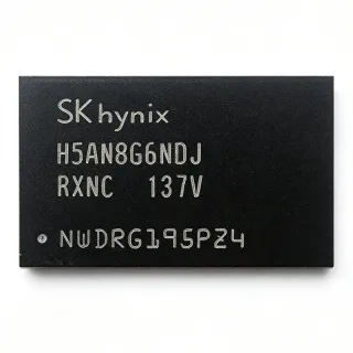
H5AN8G6NDJR-UHC - 8Gb DDR4 SDRAM 3200Mbps | SK Hynix
MPN: H5AN8G6NDJR-UHC ✓ Active| Qty | Unit Price | Extended |
|---|---|---|
| 1 | $45.11 | $45.11 |
| 10 | $42.5 | $425.00 |
| 100 | $39.8 | $3,980.00 |
| 500 | $37.2 | $18,600.00 |
| 1,000 | $34.6 | $34,600.00 |
H5AN8G6NDJR-UHC Overview
DDR4 SDRAM is the fourth generation of double data rate synchronous dynamic random-access memory, succeeding DDR3 with higher density, lower operating voltage (1.2V vs 1.5V), and improved signal integrity through on-die termination (ODT) and data bus inversion. As a volatile memory type, it stores data in capacitors that require periodic refreshing, and it transfers data on both edges of the clock signal, doubling throughput. DDR4 is the industry standard for main memory in servers, desktops, laptops, and high-performance embedded systems.
Key features include auto self-refresh, auto precharge, asynchronous reset, data mask, dynamic on-chip termination (Dynamic ODT), ZQ calibration, CRC (cyclic redundancy check), and write leveling. These features enhance signal integrity, power efficiency, and reliability in high-speed systems. The device supports a maximum operating temperature of 85°C and is lead-free and halogen-free, compliant with RoHS.
Architecturally, the H5AN8G6NDJR-UHC uses a 1x-nm class process technology, achieving high density with low power consumption. The 16-bit I/O configuration (x16) is ideal for applications requiring moderate bus width with high capacity per chip, reducing the number of devices needed on a memory module. The 96-ball FBGA package with a rectangular shape (JESD-30 code R-PBGA-B96) provides excellent thermal and electrical performance.
Typical applications include DDR4 memory modules (UDIMM, SODIMM, RDIMM), embedded computing systems, networking equipment, industrial PCs, and high-performance computing platforms. The 3200Mbps speed grade supports demanding workloads such as data analytics, virtualization, and real-time signal processing.
When designing with this device, ensure proper VDD (1.2V) and VDDQ decoupling with 0.1uF and 1uF capacitors placed close to the balls. Follow the JEDEC DDR4 layout guidelines for impedance matching and signal integrity, and use the ZQ pin with a 240-ohm resistor to ground for calibration.
Drop-in alternatives for H5AN8G6NDJR-UHC — same package, pin-to-pin compatible. Different-package parts requiring PCB rework are excluded.
Variants in this series
Same-series models that are drop-in compatible with H5AN8G6NDJR-UHC (same form factor and footprint) — differing in Package, Data Rate, Operating Temperature, Burst Length, Refresh.
Quick Comparison Tool — Select alternative parts for side-by-side comparison:
H5AN8G6NDJR-XNC
✅ Drop-In✓ In Stock
$55.6818 / Unit
View Datasheet →H5AN8G6NAFR-UHC
✅ Drop-In✓ In Stock
$5.7422 / Unit
View Datasheet →H5AN8G6NCJR-VKC
✅ Drop-In✓ In Stock
$60 / Unit
View Datasheet →K4A8G165WC-BCRC
✅ Drop-In ⚠️ Specs Unverified✓ In Stock
$23 / Unit
View Datasheet →MT40A512M16JY-075E
✅ Drop-In ⚠️ Specs Unverified✓ In Stock
$30.5 / Unit
View Datasheet →AS4C512M16D4A-62BCN
✅ Drop-In ⚠️ Specs Unverified✓ In Stock
$7.2 / Unit
View Datasheet →H5AN8G6NDJR-UHC Maximum Ratings & Electrical Characteristics
| Memory Type | DDR4 SDRAM |
| Density | 8 Gb |
| Organization | 512M x 16 |
| Speed Grade | 3200 Mbps (PC4-25600) |
| Supply Voltage (VDD) | 1.2 V |
| Supply Voltage (VDDQ) | 1.2 V |
| Number of Terminals | 96 |
| Package | FBGA-96 (13x7.5 mm) |
| Package Shape | RECTANGULAR |
| JESD-30 Code | R-PBGA-B96 |
| Maximum Operating Temperature | 85 °C |
| Minimum Operating Temperature | 0 °C |
| RoHS | Compliant |
| Lead-Free | Yes |
| Halogen Free | Yes |
| Additional Features | Auto/Self Refresh, Auto Precharge, Asynchronous Reset, Data Mask, Dynamic ODT, ZQ Calibration, CRC, Write Leveling |
H5AN8G6NDJR-UHC Pin Configuration
| Pin A1 | VDD — Power supply (1.2V) |
| Pin A2 | DQ0 — Data input/output 0 |
| Pin A3 | DQ1 — Data input/output 1 |
| Pin B1 | VSS — Ground |
| Pin B2 | DQ2 — Data input/output 2 |
| Pin B3 | DQ3 — Data input/output 3 |
| Pin C1 | VDDQ — I/O power supply (1.2V) |
| Pin C2 | DQ4 — Data input/output 4 |
| Pin C3 | DQ5 — Data input/output 5 |
| Pin D1 | VSSQ — I/O ground |
| Pin D2 | DQ6 — Data input/output 6 |
| Pin D3 | DQ7 — Data input/output 7 |
| Pin E1 | DM0 — Data mask 0 |
| Pin E2 | DQS0 — Data strobe 0 |
| Pin E3 | DQS0# — Data strobe 0 complement |
| Pin F1 | VDD — Power supply (1.2V) |
| Pin F2 | VSS — Ground |
| Pin F3 | VDDQ — I/O power supply (1.2V) |
| Pin G1 | A0 — Address input 0 |
| Pin G2 | A1 — Address input 1 |
| Pin G3 | A2 — Address input 2 |
| Pin H1 | A3 — Address input 3 |
| Pin H2 | A4 — Address input 4 |
| Pin H3 | A5 — Address input 5 |
| Pin J1 | A6 — Address input 6 |
| Pin J2 | A7 — Address input 7 |
| Pin J3 | A8 — Address input 8 |
| Pin K1 | A9 — Address input 9 |
| Pin K2 | A10/AP — Address input 10 / Auto-precharge |
| Pin K3 | A11 — Address input 11 |
| Pin L1 | A12/BC — Address input 12 / Burst chop |
| Pin L2 | A13 — Address input 13 |
| Pin L3 | A14 — Address input 14 |
| Pin M1 | A15 — Address input 15 |
| Pin M2 | A16 — Address input 16 |
| Pin M3 | BA0 — Bank address 0 |
| Pin N1 | BA1 — Bank address 1 |
| Pin N2 | BG0 — Bank group 0 |
| Pin N3 | BG1 — Bank group 1 |
| Pin P1 | CK — Clock |
| Pin P2 | CK# — Clock complement |
| Pin P3 | CKE — Clock enable |
| Pin R1 | CS# — Chip select |
| Pin R2 | ODT — On-die termination |
| Pin R3 | RAS# — Row address strobe |
| Pin T1 | CAS# — Column address strobe |
| Pin T2 | WE# — Write enable |
| Pin T3 | RESET# — Reset |
| Pin U1 | ZQ — Calibration reference |
| Pin U2 | VDD — Power supply (1.2V) |
| Pin U3 | VSS — Ground |
Typical Applications
H5AN8G6NDJR-UHC is suitable for 6 applications: Server Main Memory, Networking Equipment, Industrial PCs, High-Performance Computing, Embedded Systems, Consumer Electronics.
Server Main Memory
The H5AN8G6NDJR-UHC provides 8Gb density and 3200Mbps bandwidth, ideal for RDIMM and LRDIMM modules in servers. Its high speed supports data-intensive workloads like virtualization and cloud computing. The 1.2V operation reduces power consumption in data centers, while features like CRC and write leveling ensure reliable operation at high frequencies. When used in a dual-rank module, multiple devices can be combined to achieve capacities up to 64GB, meeting the demands of enterprise applications.
Recommended
Networking Equipment
In routers, switches, and network appliances, the H5AN8G6NDJR-UHC offers the high bandwidth needed for packet processing and routing tables. The 3200Mbps data rate enables fast lookup and forwarding, while the 8Gb density supports large routing tables and buffering. The device's low power consumption is critical for power-over-Ethernet (PoE) switches where thermal budgets are tight. Its FBGA-96 package allows compact board designs, and the auto self-refresh feature reduces standby power, extending equipment life in always-on network infrastructure.
Recommended
Industrial PCs
For industrial PCs used in automation and control, the H5AN8G6NDJR-UHC provides reliable, high-speed memory in harsh environments. With a maximum operating temperature of 85°C, it suits factory floors and outdoor installations. The 8Gb density supports complex control algorithms and data logging, while the 3200Mbps speed ensures real-time responsiveness. The device's robust design, including CRC and write leveling, maintains data integrity in electrically noisy industrial settings. Its FBGA-96 package is compatible with standard industrial motherboards, enabling easy integration.
Recommended
High-Performance Computing
In HPC clusters and workstations, the H5AN8G6NDJR-UHC delivers the memory bandwidth required for scientific simulations and data analytics. The 3200Mbps speed grade supports high-throughput computing, while the 8Gb density enables large datasets to reside in memory. The device's low latency and high reliability are essential for parallel processing workloads. Its 1.2V operation reduces power in large-scale systems, and the FBGA-96 package allows high-density DIMM designs. Features like dynamic ODT improve signal integrity at multi-GHz speeds, ensuring stable operation in demanding HPC environments.
Recommended
Embedded Systems
The H5AN8G6NDJR-UHC is suitable for high-end embedded systems such as medical imaging, military, and aerospace applications. Its 8Gb density and 3200Mbps speed support real-time image processing and complex algorithms. The device's commercial temperature range (0-85°C) is adequate for many embedded environments, and its low power consumption is beneficial for battery-powered or thermally constrained designs. The FBGA-96 package is compact, enabling small form-factor boards. Features like auto self-refresh and ZQ calibration ensure reliable operation in embedded systems with varying power conditions.
Recommended
Consumer Electronics
In high-end consumer devices like gaming PCs and workstations, the H5AN8G6NDJR-UHC provides the memory performance needed for gaming, content creation, and multitasking. The 3200Mbps speed ensures smooth frame rates and fast application loading, while the 8Gb density supports large games and creative software. The device's low power consumption is beneficial for laptops, extending battery life. Its FBGA-96 package is standard for SODIMM modules, enabling easy upgrades. Features like write leveling and dynamic ODT enhance stability in consumer systems with varying memory configurations.
Recommended
Recommended Products Summary
Engineering reference data for H5AN8G6NDJR-UHC — comparison, design guidance, and compliance information.
Selection Guide
Comparison with Alternatives
| Parameter | This Product | H5AN8G6NDJR-XNC | H5AN8G6NAFR-UHC | H5AN8G6NCJR-VKC | K4A8G165WC-BCRC | MT40A512M16JY-075E | AS4C512M16D4A-62BCN |
|---|---|---|---|---|---|---|---|
| Package | FBGA-96 (13x7.5mm) | FBGA-96 (13x7.5mm) - same | FBGA-96 (13x7.5mm) - same | FBGA-96 (13x7.5mm) - same | FBGA-96 (13x7.5mm) - same | FBGA-96 (13x7.5mm) - same | FBGA-96 (13x7.5mm) - same |
| Brand | SK Hynix | SK Hynix | SK Hynix | SK Hynix | Samsung | Micron | Alliance Memory |
| Density | 8 Gb | 8 Gb | 8 Gb | 8 Gb | 8 Gb | 8 Gb | 8 Gb |
| Organization | 512M x 16 | 512M x 16 | 512M x 16 | 512M x 16 | 512M x 16 | 512M x 16 | 512M x 16 |
| Speed Grade | 3200 Mbps | 3200 Mbps | 3200 Mbps | 2666 Mbps | 3200 Mbps | 3200 Mbps | 3200 Mbps |
| Supply Voltage | 1.2 V | 1.2 V | 1.2 V | 1.2 V | 1.2 V | 1.2 V | 1.2 V |
| Max Operating Temperature | 85 °C | 85 °C | 85 °C | 85 °C | 85 °C | 85 °C | 85 °C |
| RoHS | Compliant | Compliant | Compliant | Compliant | Compliant | Compliant | Compliant |
Key Differentiators
- Higher speed grade than VKC variant (vs H5AN8G6NCJR-VKC)
- Same-brand drop-in compatibility (vs H5AN8G6NDJR-XNC)
- Cross-brand availability (vs K4A8G165WC-BCRC)
Design Notes
Decouple VDD and VDDQ with 0.1uF and 1uF capacitors placed as close as possible to the FBGA balls. Use a solid power plane for VDD and VDDQ to minimize impedance. The 1.2V supply should be regulated within +/-5% per JEDEC DDR4 specifications. Ensure adequate bulk capacitance on the module to handle transient currents during read/write bursts.
Follow JEDEC DDR4 layout guidelines for impedance matching (typically 40-50 ohms single-ended, 80-100 ohms differential). Route DQ, DQS, and address/control signals with matched trace lengths to minimize skew. Use ground planes between signal layers to reduce crosstalk. Place the ZQ pin's 240-ohm resistor to ground close to the device, as specified in the datasheet.
Use the dynamic ODT feature to optimize signal integrity by adjusting termination impedance during reads and writes. Enable write leveling to compensate for clock-to-strobe skew. Use the CRC feature to detect data corruption on the data bus. Ensure the memory controller is configured for the correct speed grade (3200Mbps) and timing parameters from the datasheet.
Compliance Information
RoHS compliant, lead-free, and halogen-free per SK Hynix datasheet. REACH and conflict minerals status not specified in provided data.