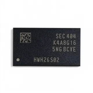
K6X0808C1D-GF55T - 32Kx8 55ns Async SRAM 5V | Samsung
부품 번호: K6X0808C1D-GF55T ✓ 활성| 수량 | 단가 | 합계 |
|---|---|---|
| 1 | $2.95 | $2.95 |
| 10 | $2.66 | $26.60 |
| 100 | $2.36 | $236.00 |
| 500 | $2.07 | $1,035.00 |
| 1,000 | $1.85 | $1,850.00 |
K6X0808C1D-GF55T 개요
An asynchronous SRAM is a type of volatile static memory that stores one bit per flip-flop cell and does not require a clock or refresh cycle, unlike DRAM. In the memory hierarchy, SRAM sits above DRAM in speed and is used wherever fast, deterministic read and write access is needed - cache memories, buffers, and embedded CPU scratchpads. Because static cells retain data while powered, asynchronous SRAMs such as this family remain popular in legacy industrial and telecom designs that need simple parallel memory interfaces.
Key features of the K6X0808C1D-GF55 include a 55 ns address access time, a single 5.0 V power supply, full-CMOS technology for low standby power, and a standard asynchronous parallel interface with dedicated chip enable (CE), output enable (OE) and write enable (WE) controls. The family supports various operating temperature ranges and multiple package types for system design flexibility, and it supports low data retention voltage for battery-backed applications.
Technically, the CMOS process yields very low power dissipation: active current is drawn only during access, and standby current drops to microamp levels in static operation. The three-wire control interface (CE, OE, WE) allows direct connection to microcontrollers, 8051-class CPUs and FPGA parallel bus logic without glue circuitry. The 32K x 8 organization maps cleanly onto a 15-bit address bus with an 8-bit data bus.
Typical applications include legacy industrial controllers, telecom line cards, network equipment buffers, test instrumentation, and battery-backed data logging in embedded systems where a simple 5 V parallel SRAM is required.
When designing with this device, ensure address setup and CE/OE timing margins meet the 55 ns access window, and add 0.1 uF decoupling near the VCC pins. Verify that the SOP-28 (450 mil) footprint is used, as the family is also offered in 28-DIP-600mil - these footprints are not interchangeable.
This page synthesizes distributor pricing, same-family drop-in alternatives, and practical design notes not found in the manufacturer datasheet.
드롭인 대체품: K6X0808C1D-GF55T — 동일 패키지, 핀 호환. PCB 재작업이 필요한 다른 패키지 부품은 제외됩니다.
이 시리즈의 변형
다음과 드롭인 호환되는 동일 시리즈 모델: K6X0808C1D-GF55T (동일 폼 팩터 및 풋프린트) — 차이점: Technology, Data Bus Width, Access Time, Memory Type, Package.
빠른 비교 도구 — 나란히 비교할 대체 부품을 선택하십시오:
K6X0808C1D-GF55T00
✅ 드롭인✓ 재고 있음
$1.05 / 개
데이터시트 보기 →K6X0808C1D-GF55000
✅ 드롭인✓ 재고 있음
$3.2 / 개
데이터시트 보기 →K6X0808C1D-GF70T00
✅ 드롭인✓ 재고 있음
$1.85 / 개
데이터시트 보기 →K6X0808C1D-GF70000
✅ 드롭인✓ 재고 있음
$1.1 / 개
데이터시트 보기 →K6X0808C1D-BF55
✅ 드롭인✓ 재고 있음
$1.85 / 개
데이터시트 보기 →K6X0808C1D-BF70T
✅ 드롭인✓ 재고 있음
$1.05 / 개
데이터시트 보기 →K6X0808C1D-GF55T 사양
| 메모리 유형 | SRAM - Asynchronous |
| 메모리 크기 | 256 Kbit |
| 메모리 구성 | 32K x 8 |
| Access Time | 55 ns |
| 공급 전압 | 5.0 V |
| 인터페이스 | Parallel |
| Process Technology | Full CMOS |
| 실장 유형 | Surface Mount |
| 패키지 | 28-SOP (450 mil) |
| Data Retention Voltage | Low data retention voltage supported (per datasheet) |
| Control Signals | CE, OE, WE |
| Address Bus Width | 15 bit |
| 데이터 버스 폭 | 8 bit |
| Packaging | Tape & Reel (T suffix) |
K6X0808C1D-GF55T 핀 구성
| 핀 1 | NC — Not connected (per datasheet) |
| 핀 2 | A0 — Address input |
| 핀 3 | A1 — Address input |
| 핀 4 | A2 — Address input |
| 핀 5 | A3 — Address input |
| 핀 6 | A4 — Address input |
| 핀 7 | A5 — Address input |
| 핀 8 | A6 — Address input |
| 핀 9 | A7 — Address input |
| 핀 10 | A8 — Address input |
| 핀 11 | A9 — Address input |
| 핀 12 | A10 — Address input |
| 핀 13 | A11 — Address input |
| 핀 14 | GND — Ground |
| 핀 15 | A12 — Address input |
| 핀 16 | A13 — Address input |
| 핀 17 | A14 — Address input |
| 핀 18 | CE — Chip enable |
| 핀 19 | DQ0 — Data input/output bit 0 |
| 핀 20 | DQ1 — Data input/output bit 1 |
| 핀 21 | DQ2 — Data input/output bit 2 |
| 핀 22 | DQ3 — Data input/output bit 3 |
| 핀 23 | WE — Write enable |
| 핀 24 | DQ4 — Data input/output bit 4 |
| 핀 25 | DQ5 — Data input/output bit 5 |
| 핀 26 | DQ6 — Data input/output bit 6 |
| 핀 27 | OE — Output enable |
| 핀 28 | DQ7 — Data input/output bit 7 |
일반적인 애플리케이션
K6X0808C1D-GF55T 적합 용도: 6 애플리케이션s: Legacy Industrial Controllers, Telecom Line Cards and Network Equipment, Battery-Backed Data Logging, Test and Measurement Instrumentation, Embedded CPU External Memory Expansion, Automotive and Marine Legacy Diagnostics Modules.
Legacy Industrial Controllers
Many industrial PLCs, motor controllers and I/O modules designed around 5 V microprocessors use external asynchronous SRAM for scratchpad and data tables. The K6X0808C1D-GF55T matches this environment directly: its single 5.0 V supply and TTL-compatible parallel interface connect to 8051-class or 80C186-class buses without level shifting or glue logic, while the 55 ns access time supports zero-wait-state cycles on slower legacy CPUs with generous margin. Its full-CMOS process keeps standby current low for control cabinets that remain powered continuously, and the low data retention voltage enables battery-backed retention of configuration and process parameters during power outages. The 28-SOP (450 mil) surface-mount package withstands industrial vibration better than DIP alternatives, and same-family speed and temperature grades allow supply-chain substitution without redesign.
추천
Telecom Line Cards and Network Equipment
Telecom line cards, T1/E1 framers and legacy network equipment frequently used 32K x 8 asynchronous SRAMs for per-channel buffers, lookup tables and statistics counters. The K6X0808C1D-GF55T fits this role with its deterministic 55 ns read/write timing - unlike DRAM, no refresh pauses interrupt service routines - and its simple CE/OE/WE control maps cleanly onto FPGA or ASIC-generated bus cycles. The 5 V CMOS interface matches the classic 5 V backplane logic common in telecom hardware. Standby power stays in the microamp range between accesses, reducing line-card thermal budget. For designs that migrated to 3.3 V, this part is only appropriate where 5 V-tolerant interfaces exist; otherwise, newer SRAM families should be evaluated. The low data retention voltage also supports redundant-store schemes in central-office equipment where configuration must survive short power interruptions.
추천
Battery-Backed Data Logging
Data loggers for energy meters, environmental sensors and industrial process recording benefit from the K6X0808C1D-GF55T's low data retention voltage: when main power fails, a small lithium backup cell can hold the 256 Kbit contents for years because CMOS static cells require almost no current to retain state. The logger's MCU writes timestamped records into the 32K x 8 array through the standard parallel bus; the dedicated WE and CE lines make write protection during power-transients straightforward by gating CE with the supervisor signal. The 55 ns access time is more than adequate for the low logging rates typical of these systems, and the 5 V supply aligns with the microcontroller rails common in field instruments. Compared with serial EEPROM solutions, this SRAM offers effectively unlimited endurance and nanosecond-scale writes for high-frequency logging.
추천
Test and Measurement Instrumentation
Bench instruments such as logic analyzers, function generators and protocol testers of the 5 V era used fast asynchronous SRAM as capture buffers and waveform memory. The K6X0808C1D-GF55T provides a 55 ns access time that supports moderate-speed capture loops, and its asynchronous nature means sample clocking is entirely under the designer's control with no refresh-induced gaps in acquired data. The 32K x 8 organization gives 32,768 8-bit samples per capture pass, sufficient for many trigger-and-display workflows. Full-CMOS construction minimizes internal heating, protecting measurement accuracy in enclosed instruments. For instrument servicing and reverse-logistics repair, this family's multiple packaging and speed grades let repair shops substitute available variants (55 ns or 70 ns) without PCB changes - an important advantage for keeping legacy test equipment in service where original parts are constrained.
추천
Embedded CPU External Memory Expansion
Microcontrollers with external bus interfaces - 8051 derivatives, Z180, H8 and similar 5 V embedded CPUs - commonly expand RAM using a single 32K x 8 SRAM. The K6X0808C1D-GF55T connects directly: 15 address lines from the CPU's address bus, 8 data lines to the multiplexed or demultiplexed data bus, and RD/WR strobes driving OE and WE, with CE derived from address decoding. At 55 ns access, the part supports zero-wait-state operation for most classic CPU clock rates, giving headroom for overclocked or margin-sensitive designs. Because the family is fabricated in full-CMOS, total system standby draw remains acceptable in always-on products. This part is a direct service replacement for failed SRAM in such products, and the same-package GF70 grade permits cost-optimized builds where one wait state is tolerable.
추천
Automotive and Marine Legacy Diagnostics Modules
Older engine management and diagnostic modules - including scan tools and 5 V ECUs - stored fault-code buffers and freeze-frame data in parallel SRAM. The K6X0808C1D-GF55T suits service and remanufacturing of such modules: its 5 V supply matches the original board rails, the 28-SOP (450 mil) footprint matches legacy layouts, and battery-backup retention via the low data retention voltage preserves trouble codes across key-off periods. For remanufacturers, availability across multiple Samsung grades (55 ns commercial, 70 ns, and BF extended-temperature variants) provides stocking flexibility when exact-speed parts are scarce, with no PCB change required. The full-CMOS process tolerates the underhood standby profiles of this equipment class when paired with proper voltage regulation. Verify the exact grade temperature rating against the module's validated environment before substitution in safety-related positions.
추천
추천 제품 요약
엔지니어링 참조 데이터: K6X0808C1D-GF55T — 비교, 설계 지침 및 규정 준수 정보.
선택 가이드
대체품과의 비교
| 파라미터 | 이 제품 | K6X0808C1D-GF55T00 | K6X0808C1D-GF70T00 | K6X0808C1D-BF55 | K6X0808C1D-BF70T |
|---|---|---|---|---|---|
| Package | 28-SOP (450 mil) | 28-SOP (450 mil) - same | 28-SOP (450 mil) - same | 28-SOP (450 mil) - same | 28-SOP (450 mil) - same |
| Brand | Samsung | Samsung | Samsung | Samsung | Samsung |
| Memory Organization | 32K x 8 (256 Kbit) | 32K x 8 (256 Kbit) | 32K x 8 (256 Kbit) | 32K x 8 (256 Kbit) | 32K x 8 (256 Kbit) |
| Access Time | 55 ns | 55 ns | 70 ns | 55 ns | 70 ns |
| Supply Voltage | 5.0 V | 5.0 V | 5.0 V | 5.0 V | 5.0 V |
| Temperature Range Grade | GF (standard) | GF (standard) | GF (standard) | BF (extended) | BF (extended) |
| Process Technology | Full CMOS | Full CMOS | Full CMOS | Full CMOS | Full CMOS |
주요 차별점
- Fastest standard speed grade in the K6X0808C1D family (vs K6X0808C1D-GF70T00)
- Standard temperature range for cost-optimized builds (vs K6X0808C1D-BF70T)
- Battery-backup friendly via low data retention voltage (vs Generic parallel SRAM equivalents)
설계 노트
Use the 28-SOP-450mil land pattern exactly as specified in the Samsung K6X0808C1D datasheet; the same family is also offered in 28-DIP-600mil, and the two footprints are NOT interchangeable. When substituting same-family variants (GF55/GF70/BF grades), verify the package outline drawing for the -T tape-and-reel suffix, as molding tolerances can vary slightly between generations. Place a 0.1 uF ceramic decoupling capacitor within 5 mm of the VCC pin, and keep address lines short and roughly length-matched to minimize skew in fast bus designs.
The device operates from a single 5.0 V rail. Estimated: with CMOS SRAM, active current is drawn primarily during access transitions, and standby current falls to microamp levels when CE is deselected - consult the datasheet ICC/ISB tables for exact values. For battery-backup designs, gate CE low during power-down with a supervisor IC so no spurious write occurs as VCC decays, and confirm the low data retention voltage threshold from the datasheet before sizing the backup cell for your required retention years.
Do not connect this 5 V SRAM directly to a 3.3 V microcontroller data bus without level shifting or confirmation of 5 V tolerance on the MCU pins - this is the most common failure mode when retrofitting legacy SRAM into modern designs. Also verify timing substitution rules: a GF70 (70 ns) part may not meet a timing budget written for 55 ns at zero wait states. Finally, tie unused address inputs only within the decoded space; never leave CE floating, or bus contention can corrupt stored data.
규정 준수 정보
Compliance data was not present in the retrieved web data for this legacy part. Verify RoHS/REACH status with Samsung Semiconductor or your distributor before specifying in new EU-market designs.