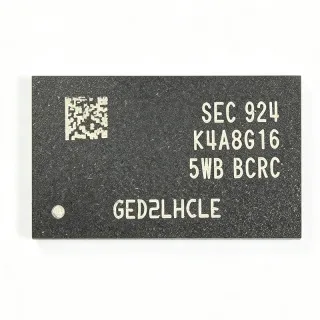
27C256A-12 - 256Kbit CMOS EPROM 32Kx8 120ns | NEC
MPN: 27C256A-12 ✗ End of Life| Qty | Unit Price | Extended |
|---|---|---|
| 1 | $3.95 | $3.95 |
| 10 | $3.56 | $35.60 |
| 100 | $3.16 | $316.00 |
| 500 | $2.84 | $1,420.00 |
| 1,000 | $2.52 | $2,520.00 |
Drop-in alternatives for 27C256A-12 — same package, pin-to-pin compatible. Different-package parts requiring PCB rework are excluded.
Quick Comparison Tool — Select alternative parts for side-by-side comparison:
27C256L-20R
✅ Drop-In✓ In Stock
$1.85 / Unit
View Datasheet →27C256T-15/SO
✅ Drop-In✓ In Stock
$1.9 / Unit
View Datasheet →27C256A12A
✅ Drop-In📋 Reference alternative (not in catalog)
27C512-20
✅ Drop-In ⚠️ 参数待验证✓ In Stock
$4.1 / Unit
View Datasheet →27C512-10
✅ Drop-In✓ In Stock
$2.7 / Unit
View Datasheet →27C256A-12 Maximum Ratings & Electrical Characteristics
| Memory Type | UV EPROM |
| Technology | CMOS |
| Memory Size | 256 Kbit (32K x 8) |
| Organization | 32K x 8 |
| Access Time | 120 ns |
| Supply Voltage (VCC) | 5 V |
| Interface | Parallel |
| Operating Temperature | 0C to +70C (commercial) |
| Package | 28-pin DIP |
| Mounting Type | Through Hole |
| Erase Method | Ultraviolet light |
| RoHS Status | unknown |
| Lifecycle Status | Obsolete (legacy product) |
27C256A-12 Pin Configuration
| Pin 1 | VPP — Programming supply voltage / program enable |
| Pin 2 | A12 — Address input |
| Pin 3 | A7 — Address input |
| Pin 4 | A6 — Address input |
| Pin 5 | A5 — Address input |
| Pin 6 | A4 — Address input |
| Pin 7 | A3 — Address input |
| Pin 8 | A2 — Address input |
| Pin 9 | A1 — Address input |
| Pin 10 | A0 — Address input |
| Pin 11 | O0 — Data output 0 |
| Pin 12 | O1 — Data output 1 |
| Pin 13 | O2 — Data output 2 |
| Pin 14 | GND — Ground |
| Pin 15 | O3 — Data output 3 |
| Pin 16 | O4 — Data output 4 |
| Pin 17 | O5 — Data output 5 |
| Pin 18 | O6 — Data output 6 |
| Pin 19 | O7 — Data output 7 |
| Pin 20 | CE — Chip enable |
| Pin 21 | A10 — Address input |
| Pin 22 | OE — Output enable |
| Pin 23 | A11 — Address input |
| Pin 24 | A9 — Address input |
| Pin 25 | A8 — Address input |
| Pin 26 | A13 — Address input |
| Pin 27 | A14 — Address input |
| Pin 28 | VCC — Power supply (5 V) |
Safe Operating Area (SOA) & Thermal Characteristics
No official SOA curve available for this digital IC. Always operate within absolute maximum ratings specified in the datasheet. Ensure adequate cooling and derate as needed.
Typical Applications
27C256A-12 is suitable for 6 applications: Embedded Firmware Storage, Retro Arcade and Console Repair, Industrial Control Equipment, Legacy BIOS and Boot Code Storage, Telecommunications Equipment, Test and Measurement Instruments.
Embedded Firmware Storage
The 27C256A-12 stores boot and application firmware for 8-bit microcontrollers and microprocessors such as the Z80, 8051, and 6809 families. Its 32K x 8 organization maps directly to a single 32 KB code space, and the 120 ns access time supports zero-wait-state fetches with most classic CPU clock speeds up to roughly 8 MHz. As a CMOS device it draws minimal standby current, an advantage in battery-backed or always-on industrial controllers. Code is burned once with a programmer and remains fixed for the product life, which suits certified or safety-adjacent equipment where field firmware changes are undesirable.
Recommended
Retro Arcade and Console Repair
Original arcade boards, home consoles, and pinball machines from the 1980s and 1990s commonly used 27C256-family EPROMs for program and graphics ROMs. The 27C256A-12, with its 120 ns access and standard DIP-28 footprint, is a preferred authentic replacement when restoring these boards. Technicians dump the original ROM, verify the CRC against known-good dumps, and program a new 27C256A-12. Because failing EPROMs exhibit bit rot after decades, replacing them with freshly programmed CMOS parts restores reliability while preserving original board aesthetics and socket compatibility.
Recommended
Industrial Control Equipment
Programmable logic controllers, motor drive controllers, and instrumentation from legacy industrial lines store their operating code in 27C256 EPROMs. The 27C256A-12 tolerates the electrically noisy industrial environment because its read-only storage is immune to corruption from power glitches, unlike RAM-based code storage. Its 5 V supply integrates directly into legacy 5 V logic rails, and the 120 ns access time meets the timing of typical 68000-family and Z180 control processors. When a controller EPROM fails, a replacement 27C256A-12 programmed from archived firmware images restores the unit to factory configuration.
Recommended
Legacy BIOS and Boot Code Storage
PC motherboards, expansion cards such as SCSI and network adapters, and single-board computers of the 286/386 era used 27C256 EPROMs to hold BIOS and option ROM code. The 27C256A-12 provides the exact 32 KB capacity of many option ROM images. Engineers maintaining or replicating vintage computing hardware use this device to reproduce authentic BIOS chips; the 120 ns access time matches ISA-bus era timing requirements. UV-erasability allows iteration during BIOS reverse-engineering or localization projects, though flash-based pin-compatible substitutes are often chosen for repeated reprogramming.
Recommended
Telecommunications Equipment
Channel banks, PBX line cards, modems, and test sets from the pre-flash era stored firmware and country-configuration tables in 27C256 EPROMs. The 27C256A-12s CMOS technology reduces power consumption across cards with dozens of memory devices, and its non-volatile read-only nature guarantees configuration integrity through power cycles. Its standard parallel interface requires no controller overhead, and the -12 speed grade accommodates the 8-16 MHz processor clocks common in telecom hardware. Service organizations keep programmed 27C256A-12 stock to field-replace firmware chips without returning cards to depots.
Recommended
Test and Measurement Instruments
Oscilloscopes, logic analyzers, and calibration fixtures from the 1990s embed 27C256 EPROMs holding self-test routines, calibration tables, and instrument firmware. The 27C256A-12 provides stable, corruption-immune storage for calibration constants that must survive decades; unlike EEPROM, its contents cannot drift under read stress. Its 120 ns access time supports the fast diagnostic sequencers used at instrument power-up. Calibration laboratories reproducing legacy instrument firmware program 27C256A-12 devices from archived images to keep discontinued test equipment serviceable, avoiding costly hardware replacement of still-accurate measurement front ends.
Recommended
Recommended Products Summary
Engineering reference data for 27C256A-12 — comparison, design guidance, and compliance information.
Selection Guide
Comparison with Alternatives
| Parameter | This Product | 27C256L-20R | 27C256T-15/SO | 27C256A12A | 27C512-10 |
|---|---|---|---|---|---|
| Package | 28-pin DIP | 28-pin DIP - same | 28-pin SOIC | 28-pin DIP - same | 28-pin DIP - same |
| Brand | NEC | Microchip Technology | Microchip Technology | NXP Semiconductors | Microchip Technology |
| Memory Size | 256 Kbit (32K x 8) | 256 Kbit (32K x 8) | 256 Kbit (32K x 8) | 256 Kbit (32K x 8) | 512 Kbit (64K x 8) |
| Access Time | 120 ns | 200 ns | 150 ns | 120 ns | 100 ns |
| Technology | CMOS | CMOS | CMOS | CMOS | CMOS |
| Supply Voltage | 5 V | 5 V | 5 V | 5 V | 5 V |
| Mounting Type | Through Hole | Through Hole | Surface Mount | Through Hole | Through Hole |
| Lifecycle Status | Obsolete | Obsolete / aftermarket | Obsolete / aftermarket | Obsolete / aftermarket | Obsolete / aftermarket |
Key Differentiators
- Fastest common speed grade in 27C256 family (vs 27C256L-20R)
- True same-speed cross-brand equivalent available (vs 27C256A12A)
- Native 32K x 8 density without address strapping (vs 27C512-10)
Design Notes
Do not assume all 27C256 devices share a programming algorithm. NEC, Philips/NXP, Microchip, and Fujitsu variants differ in VPP level (commonly 12.5 V or 21 V), program pulse width, and verify procedures. Programming a 27C256A-12 with the wrong VPP or algorithm can permanently damage the part or produce unreliable data retention. Always read the datasheet of the actual manufacturer of the specific chip in hand before programming, and verify the programmed image with a checksum or CRC read-back.
At 120 ns access time, trace delay and output loading matter in larger systems. Keep address and data traces under roughly 20 cm between the EPROM and processor, and limit each output line to a few CMOS loads to preserve the access-time budget. Decouple VCC with a 0.1 uF ceramic capacitor directly at pins 28/14. If the bus is lightly buffered, the CE-to-output access (tCE) often dominates over tAA, so check both figures against your CPU wait-state generation.
When retrofitting a 27C512 into a 27C256 socket to gain capacity or availability, strap the extra address line A15 (pin 1 on the 27C512 JEDEC pinout) appropriately: high for the upper 32K block or low for the lower block. On the 27C256 the same pin is VPP, so confirm the socket signal at pin 1 is within safe levels for the substituted device. For UV windowed parts in exposed environments, cover the window with an opaque label to prevent slow UV-induced data erasure from sunlight and fluorescent lighting.
Compliance Information
Part predates RoHS/REACH regulation and is discontinued; no compliance data is published by distributors. Repair-of-legacy-equipment exemptions may apply.