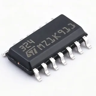
ADA4945-1ACPZ-RL7 - Low Noise FDA ADC Driver | Analog Devices
MPN: ADA4945-1ACPZ-RL7 ✓ Active| Qty | Unit Price | Extended |
|---|---|---|
| 1 | $4.85 | $4.85 |
| 10 | $4.36 | $43.60 |
| 100 | $3.88 | $388.00 |
| 500 | $3.49 | $1,745.00 |
| 1,000 | $3.1 | $3,100.00 |
ADA4945-1ACPZ-RL7 Overview
A fully differential amplifier (FDA) is an amplifier with differential inputs and differential outputs, providing balanced signals that reject common-mode noise and even-order harmonics. FDAs are essential in high-speed signal chains, particularly for driving ADCs, where they convert single-ended signals to differential, provide gain, and buffer the ADC input. The ADA4945-1 fits into the hierarchy: fully differential amplifier -> differential amplifier -> operational amplifier -> analog IC -> semiconductor.
Key features include ultra-low DC offset and offset drift (0.1 µV/°C), high speed, and excellent distortion performance. The device achieves low noise and low distortion, making it ideal for data acquisition systems requiring high accuracy. The two power modes allow a trade-off between power dissipation and bandwidth, enabling efficient operation in battery-powered or high-performance systems.
Technically, the ADA4945-1 uses a precision architecture with internal common-mode feedback, ensuring accurate output common-mode voltage control. It provides a wide input common-mode range and rail-to-rail output, simplifying interface with various ADC inputs. The device also includes a disable feature for power saving, and its small package minimizes board space.
Typical applications include driving high-speed ADCs in communications, instrumentation, and medical imaging systems. It is also used in single-ended to differential conversion, level shifting, and as a buffer for precision references. The low offset drift ensures stable performance over temperature, critical for precision measurement.
When designing with the ADA4945-1, ensure proper power supply decoupling with 0.1 µF and 10 µF capacitors close to the pins. The feedback network must be carefully matched to maintain balance and minimize distortion. The device's power mode selection should be based on the required bandwidth and power budget.
Drop-in alternatives for ADA4945-1ACPZ-RL7 — same package, pin-to-pin compatible. Different-package parts requiring PCB rework are excluded.
Variants in this series
Same-series models that are drop-in compatible with ADA4945-1ACPZ-RL7 (same form factor and footprint) — differing in Package, Power Modes.
Quick Comparison Tool — Select alternative parts for side-by-side comparison:
ADA4945-1ACPZ-R7
✅ Drop-In📋 Reference alternative (not in catalog)
ADA4945-1ACPZ-RL
✅ Drop-In📋 Reference alternative (not in catalog)
ADA4940-1ACPZ-R7
✅ Drop-In ⚠️ Specs Unverified📋 Reference alternative (not in catalog)
ADA4940-1ACPZ-RL
✅ Drop-In ⚠️ Specs Unverified📋 Reference alternative (not in catalog)
ADA4945-1ACPZ-RL7 Maximum Ratings & Electrical Characteristics
| Type | Fully Differential Amplifier |
| Supply Voltage Range | 3 V to 10 V |
| Offset Voltage Drift | 0.1 µV/°C |
| Power Modes | 2 (selectable) |
| Package | 16-LFCSP (3x3 mm) |
| Mounting Type | Surface Mount |
| RoHS Status | Compliant |
| REACH Status | Compliant |
ADA4945-1ACPZ-RL7 Pin Configuration
| Pin 1 | OUT+ — Positive differential output |
| Pin 2 | OUT- — Negative differential output |
| Pin 3 | VOCM — Output common-mode voltage control |
| Pin 4 | PD — Power-down control |
| Pin 5 | V+ — Positive supply |
| Pin 6 | IN+ — Non-inverting input |
| Pin 7 | IN- — Inverting input |
| Pin 8 | V- — Negative supply |
| Pin 9 | FB+ — Positive feedback |
| Pin 10 | FB- — Negative feedback |
| Pin 11 | GND — Ground |
| Pin 12 | NC — No connect |
Typical Applications
ADA4945-1ACPZ-RL7 is suitable for 6 applications: ADC Driver, Data Acquisition Systems, Communications Systems, Medical Imaging, Instrumentation, Test and Measurement.
ADC Driver
The ADA4945-1ACPZ-RL7 is ideal for driving high-speed ADCs. Its low noise and low distortion ensure that the ADC's performance is not degraded. The fully differential output provides balanced signals, improving common-mode rejection and reducing even-order harmonics. With a supply range of 3 V to 10 V, it can interface with various ADC supplies. The two power modes allow optimization for power-sensitive or high-performance systems. The low offset drift (0.1 µV/°C) ensures accurate conversion over temperature, making it suitable for precision data acquisition.
Recommended
Data Acquisition Systems
In data acquisition systems, the ADA4945-1ACPZ-RL7 provides the necessary signal conditioning to interface sensors with ADCs. Its low offset drift and low noise ensure accurate measurement of small signals. The device operates from 3 V to 10 V, making it compatible with a wide range of system supplies. The small LFCSP package saves board space, and the two power modes allow trade-offs between power and performance. The fully differential output helps reject common-mode interference, improving system accuracy.
Recommended
Communications Systems
The ADA4945-1ACPZ-RL7 is well-suited for communications systems, such as base stations and software-defined radios, where it drives ADCs in receive paths. Its low distortion and high linearity preserve signal integrity in the presence of strong interferers. The device's wide supply range (3 V to 10 V) accommodates various radio supply rails. The two power modes enable optimization for battery-operated or line-powered equipment. The compact package is ideal for dense PCB layouts in multi-channel systems.
Recommended
Medical Imaging
In medical imaging systems, such as ultrasound and MRI, the ADA4945-1ACPZ-RL7 is used to condition signals from transducers before ADC conversion. Its low noise and low offset drift are critical for detecting small physiological signals. The device operates from 3 V to 10 V, compatible with medical equipment power supplies. The fully differential output reduces common-mode noise, improving image quality. The small package allows high channel density in portable devices.
Recommended
Instrumentation
The ADA4945-1ACPZ-RL7 is used in precision instrumentation, such as spectrum analyzers and oscilloscopes, to drive ADCs with high accuracy. Its low offset drift (0.1 µV/°C) ensures stable measurements over temperature. The device's low noise and distortion preserve signal fidelity. The two power modes allow optimization for bench-top or portable instruments. The wide supply range (3 V to 10 V) provides flexibility in power design.
Recommended
Test and Measurement
In test and measurement equipment, the ADA4945-1ACPZ-RL7 provides signal conditioning for accurate measurements. Its low noise and low distortion are essential for high-precision testing. The device's wide supply range (3 V to 10 V) and small package make it suitable for modular instruments. The two power modes allow balancing power consumption and performance. The low offset drift ensures consistent measurements across temperature variations.
Recommended
Recommended Products Summary
Engineering reference data for ADA4945-1ACPZ-RL7 — comparison, design guidance, and compliance information.
Selection Guide
Comparison with Alternatives
| Parameter | This Product | ADA4945-1ACPZ-R7 | ADA4945-1ACPZ-RL | ADA4940-1ACPZ-R7 |
|---|---|---|---|---|
| Package | 16-LFCSP (3x3 mm) | 16-LFCSP (3x3 mm) | 16-LFCSP (3x3 mm) | 16-LFCSP (3x3 mm) |
| Brand | Analog Devices | Analog Devices | Analog Devices | Analog Devices |
| RoHS | Compliant | Compliant | Compliant | Compliant |
Key Differentiators
- Ultra-low offset drift of 0.1 µV/°C (vs ADA4940-1ACPZ-R7)
- Two selectable power modes (vs ADA4940-1ACPZ-R7)
- Broad supply range of 3 V to 10 V (vs ADA4940-1ACPZ-R7)
Design Notes
Ensure adequate power supply decoupling. Place 0.1 µF and 10 µF capacitors close to the V+ and V- pins to minimize noise and ensure stability. The ADA4945-1 operates from 3 V to 10 V, so verify the supply rails are within this range.
For optimal performance, use a solid ground plane and keep feedback paths short. Match the feedback resistor values precisely to maintain balance and minimize distortion. The LFCSP package has an exposed pad that should be soldered to the ground plane for thermal and electrical performance.
Avoid exceeding the absolute maximum supply voltage. The power mode selection should be based on the required bandwidth and power budget. Incorrect feedback network can cause instability or increased distortion. Always refer to the datasheet for recommended component values.
Compliance Information
RoHS and REACH compliant per distributor data. AEC-Q100 not applicable for this non-automotive part.