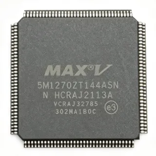
EP1C6T144LI6 - Cyclone FPGA 6K LE, 144-LQFP, Industrial | Altera
MPN: EP1C6T144LI6 ⚠ Last Time Buy| Qty | Unit Price | Extended |
|---|---|---|
| 1 | $18.5 | $18.50 |
| 10 | $16.2 | $162.00 |
| 100 | $14.1 | $1,410.00 |
| 500 | $12.4 | $6,200.00 |
| 1,000 | $11.05 | $11,050.00 |
EP1C6T144LI6 Overview
A Field Programmable Gate Array (FPGA) is a semiconductor device whose digital logic fabric, interconnect, and I/O cells can be reconfigured after manufacture by loading a user-defined bitstream into on-chip SRAM configuration memory. FPGAs sit above microcontrollers in the digital logic hierarchy, providing massively parallel hardware execution with deterministic timing, and below ASICs in terms of unit cost. Cyclone was Altera's first family optimized for low-power, low-cost applications such as consumer electronics, automotive infotainment, and industrial control, displacing CPLDs and small gate arrays in many designs. The 'T144' suffix denotes the TQFP-144 package, the 'L' suffix indicates a lead-free finish, the 'I' indicates industrial temperature range, and the '6' indicates speed grade 6.
Key features include support for up to 185 user I/O pins across four I/O banks, two dedicated phase-locked loops for clock synthesis, embedded 4-Kbit RAM blocks (M4K) for distributed buffering, support for LVDS, LVTTL, LVCMOS, SSTL-2, SSTL-3, and PCI I/O standards, and configuration via serial configuration devices, JTAG, or passive serial modes. The Cyclone architecture is built around a sea-of-LABs (Logic Array Blocks) structure with fine-grained interconnect, delivering predictable timing for synchronous designs.
The Cyclone architecture uses 4-input look-up tables (LUTs) grouped into Logic Elements (LEs), with each LE containing a register and carry chain logic for arithmetic operations. The 5,980 LEs of the EP1C6 make it suitable for moderate-complexity state machines, glue logic, bus bridges, and protocol conversion. On-chip memory of 92,160 bits is distributed across 20 M4K blocks, each capable of operating in single-port, simple dual-port, or true dual-port modes at up to 200 MHz.
Typical applications include industrial motor control, video processing front-ends, automotive telematics, consumer set-top box glue logic, telecommunications line cards, and low-cost DSP front-end processing. The combination of low unit price and high logic density made the Cyclone family a popular choice for prototyping and pre-production builds before ASIC migration.
When designing with this device, ensure that I/O bank VCCIO voltages match the signal-standard requirements (3.3V, 2.5V, 1.8V, or 1.5V) and that the dual-purpose configuration pins are correctly assigned. Use Quartus II (version 13.0 or earlier for full Cyclone support) for synthesis, place-and-route, and bitstream generation, and verify timing with TimeQuest.
This page synthesizes distributor pricing, same-brand Altera/Intel drop-in alternatives drawn from the Cyclone family, and practical design notes not consolidated in the manufacturer datasheet.
Drop-in alternatives for EP1C6T144LI6 — same package, pin-to-pin compatible. Different-package parts requiring PCB rework are excluded.
Variants in this series
Same-series models that are drop-in compatible with EP1C6T144LI6 (same form factor and footprint) — differing in Package, Family, Process Technology, Speed Grade, Total RAM Bits.
Quick Comparison Tool — Select alternative parts for side-by-side comparison:
EP1C6T144I7N
✅ Drop-In✓ In Stock
$42.5 / Unit
View Datasheet →EP1C6T144C7N
✅ Drop-In✓ In Stock
$18.4 / Unit
View Datasheet →EP1C6T144I8N
✅ Drop-In✓ In Stock
$18.75 / Unit
View Datasheet →EP1C6T144I6ES
✅ Drop-In✓ In Stock
$17.95 / Unit
View Datasheet →EP1C12T144I7N
✅ Drop-In ⚠️ Specs Unverified📋 Reference alternative (not in catalog)
EP1C20T144I7N
✅ Drop-In ⚠️ Specs Unverified📋 Reference alternative (not in catalog)
EP1C6T144LI6 Maximum Ratings & Electrical Characteristics
| Manufacturer | Altera (acquired by Intel) |
| Family | Cyclone (first-generation) |
| Logic Elements (LEs) | 5,980 |
| Process Technology | 0.13 µm SRAM |
| Total RAM Bits | 92,160 |
| Embedded RAM Blocks | 20 (M4K, 4-Kbit each) |
| Maximum User I/O Pins | 185 |
| PLLs | 2 |
| I/O Banks | 4 |
| Package | TQFP-144 (T144) |
| Speed Grade | 6 |
| Temperature Grade | Industrial (-40 °C to +100 °C TJ) |
| Configuration Modes | Passive Serial, JTAG, Altera Serial Configuration Device |
| Core Voltage (VCCINT) | 1.5 V |
| I/O Voltage (VCCIO) | 3.3 V / 2.5 V / 1.8 V / 1.5 V (bank-dependent) |
| Lead-Free Finish | Yes (per 'L' suffix) |
| Supported I/O Standards | LVTTL, LVCMOS, SSTL-2, SSTL-3, PCI, LVDS (input) |
EP1C6T144LI6 Pin Configuration
| Pin 1 | I/O — User I/O pin (Bank 1) |
| Pin 2 | I/O — User I/O pin (Bank 1) |
| Pin 3 | I/O — User I/O pin (Bank 1) |
| Pin 4 | I/O — User I/O pin (Bank 1) |
| Pin 5 | I/O — User I/O pin (Bank 1) |
| Pin 6 | VCCIO1 — I/O bank 1 supply voltage |
| Pin 7 | I/O — User I/O pin (Bank 1) |
| Pin 8 | I/O — User I/O pin (Bank 1) |
| Pin 9 | I/O — User I/O pin (Bank 1) |
| Pin 10 | GND — Ground |
| Pin 11 | I/O — User I/O pin (Bank 1) |
| Pin 12 | I/O — User I/O pin (Bank 1) |
| Pin 13 | I/O — User I/O pin (Bank 1) |
| Pin 14 | TDI — JTAG test data input |
| Pin 15 | TMS — JTAG test mode select |
| Pin 16 | TCK — JTAG test clock |
| Pin 17 | I/O — User I/O pin (Bank 1) |
| Pin 18 | I/O — User I/O pin (Bank 1) |
| Pin 19 | I/O — User I/O pin (Bank 1) |
| Pin 20 | I/O — User I/O pin (Bank 1) |
| Pin 21 | I/O — User I/O pin (Bank 1) |
| Pin 22 | I/O — User I/O pin (Bank 1) |
| Pin 23 | I/O — User I/O pin (Bank 1) |
| Pin 24 | I/O — User I/O pin (Bank 1) |
| Pin 25 | I/O — User I/O pin (Bank 1) |
| Pin 26 | I/O — User I/O pin (Bank 1) |
| Pin 27 | I/O — User I/O pin (Bank 1) |
| Pin 28 | I/O — User I/O pin (Bank 1) |
| Pin 29 | I/O — User I/O pin (Bank 1) |
| Pin 30 | I/O — User I/O pin (Bank 1) |
| Pin 31 | GND — Ground |
| Pin 32 | I/O — User I/O pin (Bank 1) |
| Pin 33 | I/O — User I/O pin (Bank 1) |
| Pin 34 | I/O — User I/O pin (Bank 1) |
| Pin 35 | I/O — User I/O pin (Bank 1) |
| Pin 36 | I/O — User I/O pin (Bank 1) |
| Pin 37 | CONF_DONE — Configuration done (open-drain) |
| Pin 38 | nSTATUS — Configuration status (open-drain) |
| Pin 39 | I/O — User I/O pin (Bank 1) |
| Pin 40 | I/O — User I/O pin (Bank 1) |
| Pin 41 | I/O — User I/O pin (Bank 1) |
| Pin 42 | I/O — User I/O pin (Bank 1) |
| Pin 43 | I/O — User I/O pin (Bank 1) |
| Pin 44 | I/O — User I/O pin (Bank 1) |
| Pin 45 | VCCIO2 — I/O bank 2 supply voltage |
| Pin 46 | I/O — User I/O pin (Bank 2) |
| Pin 47 | I/O — User I/O pin (Bank 2) |
| Pin 48 | I/O — User I/O pin (Bank 2) |
| Pin 49 | I/O — User I/O pin (Bank 2) |
| Pin 50 | I/O — User I/O pin (Bank 2) |
| Pin 51 | I/O — User I/O pin (Bank 2) |
| Pin 52 | I/O — User I/O pin (Bank 2) |
| Pin 53 | GND — Ground |
| Pin 54 | I/O — User I/O pin (Bank 2) |
| Pin 55 | I/O — User I/O pin (Bank 2) |
| Pin 56 | I/O — User I/O pin (Bank 2) |
| Pin 57 | I/O — User I/O pin (Bank 2) |
| Pin 58 | I/O — User I/O pin (Bank 2) |
| Pin 59 | I/O — User I/O pin (Bank 2) |
| Pin 60 | I/O — User I/O pin (Bank 2) |
| Pin 61 | I/O — User I/O pin (Bank 2) |
| Pin 62 | I/O — User I/O pin (Bank 2) |
| Pin 63 | I/O — User I/O pin (Bank 2) |
| Pin 64 | DCLK — Configuration clock input |
| Pin 65 | DATA0 — Configuration data input |
| Pin 66 | I/O — User I/O pin (Bank 2) |
| Pin 67 | I/O — User I/O pin (Bank 2) |
| Pin 68 | I/O — User I/O pin (Bank 2) |
| Pin 69 | I/O — User I/O pin (Bank 2) |
| Pin 70 | I/O — User I/O pin (Bank 2) |
| Pin 71 | I/O — User I/O pin (Bank 2) |
| Pin 72 | I/O — User I/O pin (Bank 2) |
| Pin 73 | GND — Ground |
| Pin 74 | I/O — User I/O pin (Bank 2) |
| Pin 75 | I/O — User I/O pin (Bank 2) |
| Pin 76 | I/O — User I/O pin (Bank 2) |
| Pin 77 | I/O — User I/O pin (Bank 2) |
| Pin 78 | I/O — User I/O pin (Bank 2) |
| Pin 79 | I/O — User I/O pin (Bank 2) |
| Pin 80 | VCCIO3 — I/O bank 3 supply voltage |
| Pin 81 | I/O — User I/O pin (Bank 3) |
| Pin 82 | I/O — User I/O pin (Bank 3) |
| Pin 83 | I/O — User I/O pin (Bank 3) |
| Pin 84 | I/O — User I/O pin (Bank 3) |
| Pin 85 | I/O — User I/O pin (Bank 3) |
| Pin 86 | I/O — User I/O pin (Bank 3) |
| Pin 87 | I/O — User I/O pin (Bank 3) |
| Pin 88 | I/O — User I/O pin (Bank 3) |
| Pin 89 | I/O — User I/O pin (Bank 3) |
| Pin 90 | I/O — User I/O pin (Bank 3) |
| Pin 91 | I/O — User I/O pin (Bank 3) |
| Pin 92 | GND — Ground |
| Pin 93 | I/O — User I/O pin (Bank 3) |
| Pin 94 | I/O — User I/O pin (Bank 3) |
| Pin 95 | I/O — User I/O pin (Bank 3) |
| Pin 96 | I/O — User I/O pin (Bank 3) |
| Pin 97 | I/O — User I/O pin (Bank 3) |
| Pin 98 | I/O — User I/O pin (Bank 3) |
| Pin 99 | I/O — User I/O pin (Bank 3) |
| Pin 100 | I/O — User I/O pin (Bank 3) |
| Pin 101 | I/O — User I/O pin (Bank 3) |
| Pin 102 | I/O — User I/O pin (Bank 3) |
| Pin 103 | I/O — User I/O pin (Bank 3) |
| Pin 104 | I/O — User I/O pin (Bank 3) |
| Pin 105 | I/O — User I/O pin (Bank 3) |
| Pin 106 | I/O — User I/O pin (Bank 3) |
| Pin 107 | I/O — User I/O pin (Bank 3) |
| Pin 108 | I/O — User I/O pin (Bank 3) |
| Pin 109 | I/O — User I/O pin (Bank 3) |
| Pin 110 | I/O — User I/O pin (Bank 3) |
| Pin 111 | GND — Ground |
| Pin 112 | VCCIO4 — I/O bank 4 supply voltage |
| Pin 113 | I/O — User I/O pin (Bank 4) |
| Pin 114 | I/O — User I/O pin (Bank 4) |
| Pin 115 | I/O — User I/O pin (Bank 4) |
| Pin 116 | I/O — User I/O pin (Bank 4) |
| Pin 117 | I/O — User I/O pin (Bank 4) |
| Pin 118 | I/O — User I/O pin (Bank 4) |
| Pin 119 | I/O — User I/O pin (Bank 4) |
| Pin 120 | I/O — User I/O pin (Bank 4) |
| Pin 121 | I/O — User I/O pin (Bank 4) |
| Pin 122 | I/O — User I/O pin (Bank 4) |
| Pin 123 | I/O — User I/O pin (Bank 4) |
| Pin 124 | I/O — User I/O pin (Bank 4) |
| Pin 125 | I/O — User I/O pin (Bank 4) |
| Pin 126 | I/O — User I/O pin (Bank 4) |
| Pin 127 | I/O — User I/O pin (Bank 4) |
| Pin 128 | I/O — User I/O pin (Bank 4) |
| Pin 129 | I/O — User I/O pin (Bank 4) |
| Pin 130 | I/O — User I/O pin (Bank 4) |
| Pin 131 | I/O — User I/O pin (Bank 4) |
| Pin 132 | I/O — User I/O pin (Bank 4) |
| Pin 133 | GND — Ground |
| Pin 134 | I/O — User I/O pin (Bank 4) |
| Pin 135 | I/O — User I/O pin (Bank 4) |
| Pin 136 | I/O — User I/O pin (Bank 4) |
| Pin 137 | I/O — User I/O pin (Bank 4) |
| Pin 138 | I/O — User I/O pin (Bank 4) |
| Pin 139 | I/O — User I/O pin (Bank 4) |
| Pin 140 | I/O — User I/O pin (Bank 4) |
| Pin 141 | VCCINT — Core supply voltage (1.5 V) |
| Pin 142 | I/O — User I/O pin (Bank 4) |
| Pin 143 | I/O — User I/O pin (Bank 4) |
| Pin 144 | I/O — User I/O pin (Bank 4) |
Typical Applications
EP1C6T144LI6 is suitable for 6 applications: Industrial Motor Control, Video Processing Front-End, Automotive Infotainment Glue Logic, Consumer Set-Top Box Interface Bridge, Telecommunications Line Card Glue Logic, Low-Cost DSP Pre-Processing Front-End.
Industrial Motor Control
The EP1C6T144LI6 fits industrial motor-control boards because its 5,980 LEs comfortably host PWM generation, Hall-sensor decoding, and PI/DTC control loops for a single 3-phase BLDC or stepper drive, while the 185 user I/O pins of the TQFP-144 package accommodate gate-driver interfaces, encoder inputs, and fault-monitoring signals. Two PLLs derive the PWM switching clock (typically 20-50 kHz) and the control-loop sample clock from a single 50 MHz crystal, eliminating the need for multiple oscillators on the PCB. Compared with an MCU-based design, the parallel hardware execution of the FPGA allows deterministic sub-microsecond loop times, which directly improves torque ripple and current-loop bandwidth. Industrial temperature grade (-40 to +100 °C TJ) supports factory-floor operation without derating. Companion parts include the EPC3 EPCS configuration memory and the IR2104 gate driver.
Recommended
Video Processing Front-End
The EP1C6T144LI6 is well matched to video front-end tasks such as NTSC/PAL decoding, image scaling, de-interlacing, and on-screen display overlay, where 5,980 LEs and 92,160 bits of on-chip RAM are sufficient for one or two video pipelines. The M4K blocks configured as line buffers hold a full video line of pixel data, eliminating external SRAM for many designs. LVDS input support on the FPGA's differential pairs (in TQFP-144) allows direct interface to digital camera or HDMI front-end receivers without external deserializers. Quartus II reference designs and Altera application notes provide ready-to-use IP for color-space conversion and gamma correction. Companion parts include the ADV7180 video decoder and the EPCS16 configuration memory.
Recommended
Automotive Infotainment Glue Logic
The EP1C6T144LI6 served as cost-effective glue logic in automotive infotainment head units, bridging I2S audio buses, CAN/LIN vehicle networks, SPI display controllers, and custom keypad matrices. With 5,980 LEs and 185 I/O pins, the FPGA absorbs protocol-translation, format conversion, and timing-management tasks that would otherwise require multiple CPLDs and bus-switch ICs, reducing BOM cost and PCB area. Two PLLs generate the audio-master clock (commonly 12.288 MHz for 48 kHz sample rates) and the display pixel clock from a single reference. Industrial temperature grade was sufficient for cabin-mounted head units in early 2000s designs. Companion parts include the TJA1050 CAN transceiver and the PCM5101A audio DAC.
Recommended
Consumer Set-Top Box Interface Bridge
The EP1C6T144LI6 implements bus-format bridges in set-top boxes, converting between parallel processor buses, IDE/ATA storage interfaces, and serial transport streams such as DVB or ATSC. Its 5,980 LEs are sufficient for TS demultiplexing, PID filtering, and encryption key insertion at line rates. On-chip M4K RAM blocks provide the small packet-buffer FIFOs needed between MPEG and host-CPU interfaces, removing the need for external SRAM. Low unit cost made Cyclone the dominant choice for mid-volume consumer STB designs from 2003-2008. Companion parts include the M29W320DB flash memory and the LNBH23 LNB supply controller.
Recommended
Telecommunications Line Card Glue Logic
The EP1C6T144LI6 acts as timing-and-control glue logic on telecom line cards, providing TDM bus formatting, framing, alarm-collection, and clock-distribution functions for 4-8 E1/T1 or 1-2 E3/DS3 ports. Two PLLs derive multiple clock rates (2.048 MHz E1, 8.192 MHz, 44.736 MHz DS3) from a single board reference oscillator with sub-ppm jitter. LVTTL/LVCMOS I/O standards and high pin count of the TQFP-144 package accommodate backplane interface needs. Quartus II timing closure with TimeQuest analysis supports the deterministic sub-microsecond framing and slip-buffer requirements of telecom equipment. Companion parts include the DS21348 LIU and the IDT72V36100 FIFO.
Recommended
Low-Cost DSP Pre-Processing Front-End
The EP1C6T144LI6 implements the FPGA co-processor pattern widely used in mid-2000s DSP systems, off-loading FIR filters, FFT pre-processing, and data-rate conversion from a host DSP such as the TI TMS320C6000 series. With 5,980 LEs, the Cyclone can host a 32-tap FIR at 100 MHz sample rate, or a 256-point radix-2 FFT pipeline, while the 92,160 bits of M4K memory hold coefficient and twiddle tables without external ROM. The dual-port RAM mode of M4K blocks enables simultaneous coefficient read and data write operations required for streaming DSP. Quartus II MegaWizard plug-ins (now Platform Designer) generate ready-to-use FIR and FFT IP. Companion parts include the TMS320C6713 DSP and the AD9244 ADC.
Recommended
Recommended Products Summary
Engineering reference data for EP1C6T144LI6 — comparison, design guidance, and compliance information.
Selection Guide
Comparison with Alternatives
| Parameter | This Product | EP1C6T144I7N | EP1C6T144C7N | EP1C6T144I8N | EP1C12T144I7N | EP1C20T144I7N |
|---|---|---|---|---|---|---|
| Brand | Altera | Altera | Altera | Altera | Altera | Altera |
| Package | TQFP-144 | TQFP-144 (same) | TQFP-144 (same) | TQFP-144 (same) | TQFP-144 (same) | TQFP-144 (same) |
| Logic Elements | 5,980 | 5,980 (same) | 5,980 (same) | 5,980 (same) | 12,060 (+101%) | 20,060 (+235%) |
| Total RAM Bits | 92,160 | 92,160 (same) | 92,160 (same) | 92,160 (same) | 239,616 (+160%) | 294,912 (+220%) |
| Speed Grade | 6 | 7 (faster) | 7 (faster) | 8 (fastest) | 7 (faster) | 7 (faster) |
| Temperature Grade | Industrial (-40 to +100C TJ) | Industrial (same) | Commercial (0 to +85C TJ) | Industrial (same) | Industrial (same) | Industrial (same) |
| PLLs | 2 | 2 (same) | 2 (same) | 2 (same) | 2 (same) | 2 (same) |
| Max User I/O | 185 | 185 (same) | 185 (same) | 185 (same) | 249 (TQFP-144 layout dependent) | 252 (TQFP-144 layout dependent) |
| Lead-Free | Yes (L suffix) | Yes (N suffix) | Yes (N suffix) | Yes (N suffix) | Yes (N suffix) | Yes (N suffix) |
Key Differentiators
- Faster speed grade 7 (vs 6) on identical die and footprint (vs EP1C6T144I7N)
- Doubles logic density with pin-compatible footprint (vs EP1C12T144I7N)
- Maximum timing headroom in the Cyclone family (speed grade 8) (vs EP1C6T144I8N)
Design Notes
Estimated: total power consumption for the EP1C6T144LI6 typical application is approximately 0.5-1.5 W depending on utilization and toggle rate. Use the Altera PowerPlay Early Power Estimator (EPE) spreadsheet with assumed parameters (LEs used: ~70%, RAM blocks: ~50%, toggle rate: 12.5%, clock frequency: 100 MHz) to refine the budget. Decouple VCCINT (1.5 V) with one 100 µF bulk + four 0.1 µF ceramic capacitors placed adjacent to package power pins (141, plus distributed across the die area) to limit switching-noise ripple below 50 mV peak-to-peak.
Do not omit pull-up resistors on the open-drain configuration pins CONF_DONE (pin 37) and nSTATUS (pin 38); both require 10 kΩ pull-ups to VCCIO of the bank containing the configuration pins. Failure to pull these up causes configuration failure on power-up with the typical Active Serial (AS) or Passive Serial (PS) configuration schemes. Also verify that dual-purpose configuration pins (DATA0, DCLK) are assigned correctly in the Quartus II pin planner so that they revert to user I/O when configuration completes.
The TQFP-144 package of the EP1C6T144LI6 requires a 4-layer PCB minimum, with one continuous ground plane beneath the package and a VCCINT island on the top layer for direct capacitor attachment. Trace impedance for high-speed I/O (such as LVDS inputs or memory interfaces) should be controlled to 50 Ω single-ended or 100 Ω differential. Maintain 3W spacing between high-speed signals (clocks, DCLK, DATA[7:0] in PS mode) and adjacent user I/O traces to minimize crosstalk; Altera application note AN224 provides detailed Cyclone layout guidelines.
Compliance Information
RoHS compliant per the 'L' suffix in the part number indicating lead-free finish; industrial temperature grade is not AEC-Q100 qualified - for automotive applications migrate to Cyclone III/IV automotive-grade parts.