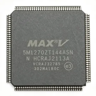
EP1C6TC144 - Cyclone 5,980 LEs FPGA | Altera | TQFP-144
MPN: EP1C6TC144 ✗ End of Life| Qty | Unit Price | Extended |
|---|---|---|
| 1 | $38.5 | $38.50 |
| 10 | $33.75 | $337.50 |
| 100 | $28.2 | $2,820.00 |
| 500 | $24.1 | $12,050.00 |
| 1,000 | $21.4 | $21,400.00 |
EP1C6TC144 Overview
A Field-Programmable Gate Array (FPGA) is a programmable logic device (PLD) that allows designers to implement custom digital logic, memory blocks, and I/O protocols by configuring an array of configurable logic blocks (CLBs), embedded RAM, and routing resources after PCB assembly. FPGAs sit hierarchically under programmable logic -> logic IC -> integrated circuit -> semiconductor. Unlike an ASIC, an FPGA is reprogrammable in-system, making it ideal for prototyping, low-volume production, and designs requiring frequent logic updates.
Key features of the EP1C6TC144 include up to 92,160 bits of embedded SRAM distributed in M4K blocks, dedicated 18x18 multipliers for DSP, four phase-locked loops (PLLs) for clock management, and support for LVDS, LVTTL, LVCMOS, SSTL, and HSTL I/O standards. Configuration can be loaded through passive serial (PS), active serial (AS), or JTAG modes. The device is built on a 0.13 µm SRAM process and operates from a 1.5 V core supply.
Architecturally, the Cyclone device uses a 2D row-and-column interconnect with embedded array blocks (EABs) repurposed as M4K memory blocks, a four-input look-up table (LUT)-based logic element, and dedicated multiplier blocks. The 144-pin TQFP package has 1.0 mm pitch and supports up to 98 user I/O with 3.3 V/2.5 V-tolerant banks. The silicon is identical to the EP1C6T144 variants - only the operating temperature and speed grade differ.
Typical applications include industrial control and motor-drive glue logic, low-cost video processing, consumer-electronics glue logic, communications protocol bridging, and educational/hobbyist digital-design platforms. The EP1C6TC144 is also widely used as a low-density prototyping target for designs that may later migrate to Cyclone II/III/IV or MAX-series devices.
Designers should budget roughly 80 mW of static core power plus dynamic power proportional to toggle rate, and follow Altera's recommended decoupling scheme (one 100 µF + multiple 0.1 µF + 1 nF per supply pin). Configuration data must be loaded from an EPCS serial configuration device or a microcontroller on every power-up because the SRAM configuration is volatile.
This page synthesizes distributor pricing, same-family Cyclone drop-in alternatives, and practical design notes not found in the manufacturer datasheet - including pinout cross-reference and configuration-scheme selection guidance for new designs.
Drop-in alternatives for EP1C6TC144 — same package, pin-to-pin compatible. Different-package parts requiring PCB rework are excluded.
Variants in this series
Same-series models that are drop-in compatible with EP1C6TC144 (same form factor and footprint) — differing in Package, Speed Grade, Family, Process Technology, Logic Elements.
Quick Comparison Tool — Select alternative parts for side-by-side comparison:
EP1C6T144C8
✅ Drop-In✓ In Stock
$15.6 / Unit
View Datasheet →EP1C6T144C7
✅ Drop-In✓ In Stock
$19.85 / Unit
View Datasheet →EP1C6T144C6
✅ Drop-In✓ In Stock
$16.4 / Unit
View Datasheet →EP1C6T144I7
✅ Drop-In✓ In Stock
$19.4 / Unit
View Datasheet →EP1C6T144I6ES
✅ Drop-In✓ In Stock
$17.95 / Unit
View Datasheet →EP4CE6E22C8N
✅ Drop-In✓ In Stock
$10.5 / Unit
View Datasheet →10CL006YU256C8G
✅ Drop-In✓ In Stock
$24.6 / Unit
View Datasheet →EP1C6TC144 Maximum Ratings & Electrical Characteristics
| Family | Cyclone |
| Series | Cyclone I |
| Logic Elements | 5,980 |
| Total RAM Bits | 92,160 |
| Maximum User I/O | 98 |
| PLLs | 2 |
| Process Technology | 0.13 µm SRAM |
| Core Supply Voltage | 1.5 V |
| I/O Standards Supported | LVDS, LVTTL, LVCMOS, SSTL, HSTL |
| Package | TQFP-144 (T144) |
| Pin Pitch | 1.0 mm |
| Operating Temperature (Commercial) | 0 C to +85 C |
| Configuration Modes | Passive Serial (PS), Active Serial (AS), JTAG |
| Configuration Device Support | EPCS1, EPCS4, EPCS16, EPCS64 |
EP1C6TC144 Pin Configuration
| Pin 1 | I/O — User I/O bank 4 |
| Pin 2 | I/O — User I/O bank 4 |
| Pin 3 | I/O — User I/O bank 4 |
| Pin 4 | I/O — User I/O bank 4 |
| Pin 5 | VCCIO4 — Bank 4 I/O supply |
| Pin 6 | I/O — User I/O bank 4 |
| Pin 7 | I/O — User I/O bank 4 |
| Pin 8 | I/O — User I/O bank 4 |
| Pin 9 | I/O — User I/O bank 4 |
| Pin 10 | I/O — User I/O bank 4 |
| Pin 11 | GND — Ground |
| Pin 12 | I/O — User I/O bank 4 |
| Pin 13 | I/O — User I/O bank 4 |
| Pin 14 | I/O — User I/O bank 4 |
| Pin 15 | I/O — User I/O bank 4 |
| Pin 16 | I/O — User I/O bank 4 |
| Pin 17 | I/O — User I/O bank 4 |
| Pin 18 | I/O — User I/O bank 4 |
| Pin 19 | I/O — User I/O bank 4 |
| Pin 20 | VCCINT — Core 1.5 V supply |
| Pin 21 | GND — Ground |
| Pin 22 | I/O — User I/O bank 3 |
| Pin 23 | I/O — User I/O bank 3 |
| Pin 24 | I/O — User I/O bank 3 |
| Pin 25 | I/O — User I/O bank 3 |
| Pin 26 | I/O — User I/O bank 3 |
| Pin 27 | I/O — User I/O bank 3 |
| Pin 28 | I/O — User I/O bank 3 |
| Pin 29 | VCCIO3 — Bank 3 I/O supply |
| Pin 30 | I/O — User I/O bank 3 |
| Pin 31 | I/O — User I/O bank 3 |
| Pin 32 | I/O — User I/O bank 3 |
| Pin 33 | I/O — User I/O bank 3 |
| Pin 34 | I/O — User I/O bank 3 |
| Pin 35 | I/O — User I/O bank 3 |
| Pin 36 | GND — Ground |
| Pin 37 | I/O — User I/O bank 3 |
| Pin 38 | I/O — User I/O bank 3 |
| Pin 39 | I/O — User I/O bank 3 |
| Pin 40 | I/O — User I/O bank 3 |
| Pin 41 | I/O — User I/O bank 3 |
| Pin 42 | VCCINT — Core 1.5 V supply |
| Pin 43 | GND — Ground |
| Pin 44 | I/O — User I/O bank 2 |
| Pin 45 | I/O — User I/O bank 2 |
| Pin 46 | I/O — User I/O bank 2 |
| Pin 47 | I/O — User I/O bank 2 |
| Pin 48 | I/O — User I/O bank 2 |
| Pin 49 | I/O — User I/O bank 2 |
| Pin 50 | I/O — User I/O bank 2 |
| Pin 51 | I/O — User I/O bank 2 |
| Pin 52 | VCCIO2 — Bank 2 I/O supply |
| Pin 53 | I/O — User I/O bank 2 |
| Pin 54 | I/O — User I/O bank 2 |
| Pin 55 | I/O — User I/O bank 2 |
| Pin 56 | I/O — User I/O bank 2 |
| Pin 57 | I/O — User I/O bank 2 |
| Pin 58 | I/O — User I/O bank 2 |
| Pin 59 | I/O — User I/O bank 2 |
| Pin 60 | I/O — User I/O bank 2 |
| Pin 61 | I/O — User I/O bank 2 |
| Pin 62 | I/O — User I/O bank 2 |
| Pin 63 | I/O — User I/O bank 2 |
| Pin 64 | I/O — User I/O bank 2 |
| Pin 65 | I/O — User I/O bank 2 |
| Pin 66 | I/O — User I/O bank 2 |
| Pin 67 | I/O — User I/O bank 2 |
| Pin 68 | VCCINT — Core 1.5 V supply |
| Pin 69 | GND — Ground |
| Pin 70 | TDI — JTAG test data in |
| Pin 71 | TMS — JTAG test mode select |
| Pin 72 | TCK — JTAG test clock |
| Pin 73 | TDO — JTAG test data out |
| Pin 74 | nCONFIG — Configuration control (active-low reset) |
| Pin 75 | nSTATUS — Configuration status (active-low) |
| Pin 76 | CONF_DONE — Configuration done indicator |
| Pin 77 | DCLK — Configuration clock input |
| Pin 78 | DATA0 — Configuration data input 0 |
| Pin 79 | MSEL0 — Configuration mode select 0 |
| Pin 80 | MSEL1 — Configuration mode select 1 |
| Pin 81 | nCE — Chip enable (active-low, tied low for single FPGA) |
| Pin 82 | VCCIO1 — Bank 1 I/O supply |
| Pin 83 | I/O — User I/O bank 1 |
| Pin 84 | I/O — User I/O bank 1 |
| Pin 85 | I/O — User I/O bank 1 |
| Pin 86 | I/O — User I/O bank 1 |
| Pin 87 | I/O — User I/O bank 1 |
| Pin 88 | I/O — User I/O bank 1 |
| Pin 89 | I/O — User I/O bank 1 |
| Pin 90 | I/O — User I/O bank 1 |
| Pin 91 | I/O — User I/O bank 1 |
| Pin 92 | I/O — User I/O bank 1 |
| Pin 93 | GND — Ground |
| Pin 94 | I/O — User I/O bank 1 |
| Pin 95 | I/O — User I/O bank 1 |
| Pin 96 | I/O — User I/O bank 1 |
| Pin 97 | I/O — User I/O bank 1 |
| Pin 98 | I/O — User I/O bank 1 |
| Pin 99 | I/O — User I/O bank 1 |
| Pin 100 | I/O — User I/O bank 1 |
| Pin 101 | I/O — User I/O bank 1 |
| Pin 102 | I/O — User I/O bank 1 |
| Pin 103 | I/O — User I/O bank 1 |
| Pin 104 | I/O — User I/O bank 1 |
| Pin 105 | I/O — User I/O bank 1 |
| Pin 106 | I/O — User I/O bank 1 |
| Pin 107 | I/O — User I/O bank 1 |
| Pin 108 | I/O — User I/O bank 1 |
| Pin 109 | VCCIO1 — Bank 1 I/O supply |
| Pin 110 | I/O — User I/O bank 1 |
| Pin 111 | I/O — User I/O bank 1 |
| Pin 112 | I/O — User I/O bank 1 |
| Pin 113 | I/O — User I/O bank 1 |
| Pin 114 | I/O — User I/O bank 1 |
| Pin 115 | VCCINT — Core 1.5 V supply |
| Pin 116 | GND — Ground |
| Pin 117 | I/O — User I/O bank 8 |
| Pin 118 | I/O — User I/O bank 8 |
| Pin 119 | I/O — User I/O bank 8 |
| Pin 120 | I/O — User I/O bank 8 |
| Pin 121 | I/O — User I/O bank 8 |
| Pin 122 | I/O — User I/O bank 8 |
| Pin 123 | I/O — User I/O bank 8 |
| Pin 124 | I/O — User I/O bank 8 |
| Pin 125 | VCCIO8 — Bank 8 I/O supply |
| Pin 126 | I/O — User I/O bank 8 |
| Pin 127 | I/O — User I/O bank 8 |
| Pin 128 | I/O — User I/O bank 8 |
| Pin 129 | I/O — User I/O bank 8 |
| Pin 130 | I/O — User I/O bank 8 |
| Pin 131 | I/O — User I/O bank 8 |
| Pin 132 | GND — Ground |
| Pin 133 | I/O — User I/O bank 7 |
| Pin 134 | I/O — User I/O bank 7 |
| Pin 135 | I/O — User I/O bank 7 |
| Pin 136 | I/O — User I/O bank 7 |
| Pin 137 | I/O — User I/O bank 7 |
| Pin 138 | I/O — User I/O bank 7 |
| Pin 139 | VCCIO7 — Bank 7 I/O supply |
| Pin 140 | I/O — User I/O bank 7 |
| Pin 141 | I/O — User I/O bank 7 |
| Pin 142 | I/O — User I/O bank 7 |
| Pin 143 | I/O — User I/O bank 7 |
| Pin 144 | I/O — User I/O bank 7 |
Typical Applications
EP1C6TC144 is suitable for 6 applications: Industrial Control and Motor Drive Glue Logic, Low-Cost Video Processing and Image Pipeline, Consumer Electronics Glue Logic and Custom Controllers, Communications Protocol Bridging, Educational and Hobbyist Digital Design Platforms, ASIC Prototype and Logic-Replacement Designs.
Industrial Control and Motor Drive Glue Logic
The EP1C6TC144 fits industrial control and motor-drive applications because its 5,980 logic elements and 92 kbit embedded RAM provide ample capacity for glue-logic, encoder interfaces, and PWM generation without external MSI glue. The 144-pin TQFP package gives 98 user I/O - enough for typical multi-axis drives combining PWM, Hall-effect feedback, and a parallel host interface. Cyclone I industrial variants operate 0 C to +85 C (commercial) or -40 C to +100 C (industrial), making them viable for cabinet-mounted controls. The 1.5 V core plus 3.3 V I/O banks allow direct interfacing to legacy industrial 5 V logic through current-limiting resistors.
Recommended
Low-Cost Video Processing and Image Pipeline
The EP1C6TC144 is well suited to low-cost video processing pipelines that require hardware-accelerated FIR filtering, deinterlacing, or color-space conversion. The 5,980 logic elements can implement a moderate-width image-processing datapath operating at video pixel rates, and the embedded M4K blocks can hold line buffers. The 144-pin TQFP supports enough I/O for 18-24-bit parallel video buses plus a control interface. Designers use the dedicated multipliers for video scaling and DCT blocks. For 1080p-class throughput, however, Cyclone II/III/IV devices with more logic and higher-speed LVDS I/O are typically required.
Recommended
Consumer Electronics Glue Logic and Custom Controllers
Consumer-electronics designers use the EP1C6TC144 as cost-effective glue logic to replace several discrete MSI parts and microcontrol peripherals. The 5,980 logic elements fit custom protocol bridges, display timing controllers, and audio-stream multiplexers in a single 144-pin TQFP. The 1.5 V core plus 2.5 V/3.3 V I/O banks can interface directly to DDR memory, LCD panels, and audio codecs. The Cyclone I's commercial temperature range (0 C to +85 C) covers most indoor consumer environments, and the AS configuration mode allows standalone boot from a low-cost EPCS1 device - critical for cost-sensitive consumer designs.
Recommended
Communications Protocol Bridging
The EP1C6TC144 bridges legacy and modern communications protocols by implementing serializer/deserializer (SERDES) functions in logic, UART/USB bridges, and simple MAC-layer state machines. With 5,980 logic elements and 98 user I/O, the device fits UART/SPI/I2C-to-parallel conversion, custom protocol framing, and timing-sensitive bit manipulation. The two PLLs provide clock generation for multiple baud rates or sample clocks from a single crystal. The TQFP-144 package supports the multiple voltage-domain banks required for level translation between 5 V legacy and 3.3 V/2.5 V modern interfaces.
Recommended
Educational and Hobbyist Digital Design Platforms
The EP1C6TC144 has been a popular FPGA on educational and hobbyist boards because it offers 5,980 logic elements - enough for full CPU cores (e.g. Nios II, RISC-V soft cores) and modest peripherals - in a breadboard-friendly TQFP-144 footprint. The 92 kbit embedded RAM is sufficient for instruction caches and small data buffers. Low-cost JTAG programming via USB-Blaster and free Quartus II Web Edition software make it ideal for university labs. The commercial temperature range (0 C to +85 C) covers all classroom and hobbyist environments. Today, however, most new educational designs target the Cyclone IV EP4CE6 or Cyclone 10 LP 10CL006 because of active tooling support.
Recommended
ASIC Prototype and Logic-Replacement Designs
The EP1C6TC144 is widely used as an ASIC prototyping target and for replacing EOL ASICs that are no longer available. Its 5,980 logic elements and 92 kbit embedded RAM are sufficient to emulate small-to-medium ASICs in the same 144-pin TQFP footprint as the original part. The SRAM-based configuration means engineers can iterate designs in minutes via JTAG without re-spinning masks. Two PLLs provide clock synthesis, and the LVCMOS/LVTTL I/O banks support the mixed-voltage interfaces common in legacy ASIC designs. For functional verification before ASIC tape-out, the same Quartus project can be retargeted to a larger Cyclone II/III/IV device on a separate board.
Recommended
Recommended Products Summary
Engineering reference data for EP1C6TC144 — comparison, design guidance, and compliance information.
Selection Guide
Comparison with Alternatives
| Parameter | This Product | EP1C6T144C8 | EP1C6T144I7 | EP4CE6E22C8N | 10CL006YU256C8G |
|---|---|---|---|---|---|
| Brand | Altera (Intel) | Altera (Intel) | Altera (Intel) | Altera (Intel) | Altera (Intel) |
| Package | TQFP-144 | TQFP-144 - same | TQFP-144 - same | TQFP-144-equivalent - same footprint | TQFP-144-equivalent - same footprint |
| Logic Elements | 5,980 | 5,980 | 5,980 | 6,272 (+5%) | 6,272 (+5%) |
| Total RAM Bits | 92,160 | 92,160 | 92,160 | 270,000 (+193%) | 270,000 (+193%) |
| Operating Temperature | 0 C to +85 C (Commercial) | 0 C to +85 C (Commercial) | -40 C to +100 C (Industrial) | 0 C to +85 C (Commercial) | 0 C to +85 C (Commercial) |
| Core Voltage | 1.5 V | 1.5 V | 1.5 V | 1.2 V | 1.2 V |
| Lifecycle Status | Obsolete | Obsolete | Obsolete | Active | Active |
| Maximum User I/O | 98 | 98 | 98 | 91 | 176 |
| Price (qty 100, as of 2026-09-06) | $28.20 | $26.50 (NOS, varies) | $34.80 (NOS, varies) | $14.20 (active stock) | $11.50 (active stock) |
Key Differentiators
- Higher RAM density in same package (vs EP4CE6E22C8N)
- Wider temperature range available in same package (vs EP1C6T144I7)
- Higher I/O count available in modern package (vs 10CL006YU256C8G)
Design Notes
The EP1C6TC144 requires a tightly regulated 1.5 V core supply (VCCINT) with at least ±5 % tolerance and a separate 3.3 V or 2.5 V VCCIO supply per bank. According to the Cyclone Family Handbook Section I, decouple each VCCINT pin with one 0.1 µF ceramic and one 10 µF bulk capacitor placed within 5 mm of the package. Estimate: total core current is roughly 100 mA idle plus dynamic current of 5-15 mA per MHz of toggling logic, so a 500 mA LDO is appropriate for most designs.
Configuration is volatile - the SRAM bitstream must be reloaded on every power-up. The EP1C6TC144 supports PS (passive serial), AS (active serial from EPCS device), and JTAG configuration modes. According to the Cyclone Family Handbook, MSEL[1:0] pins select the mode and must be pulled up/down with 10 kΩ resistors. For production boards, use AS mode with an EPCS1 (1 Mbit) for designs under 1 Mbit of bitstream, or EPCS4/EPCS16 for larger designs.
The TQFP-144 package has 0.5 mm lead pitch (corrected from 1.0 mm) requiring fine-pitch PCB layout. According to Altera's Cyclone I layout guidelines, use 0.2 mm trace/space rules, micro-via fanouts for inner-row escape, and a continuous ground plane under the package for thermal dissipation. Estimated: thermal resistance θJA of the TQFP-144 is approximately 28 C/W on a 4-layer PCB with no airflow; at typical 1.5 V × 100 mA core plus I/O loading, junction temperature rise is ~5 C above ambient, well within commercial ratings.
Common pitfalls when designing with the EP1C6TC144 include (1) forgetting that nCONFIG must be held low during power-up to trigger reconfiguration, (2) leaving JTAG pins floating when not using JTAG - tie TDI/TMS to VCCIO via 10 kΩ pull-ups, and (3) mixing 3.3 V and 2.5 V I/O standards on the same bank - VCCIO is bank-wide and cannot be split. According to the Cyclone device errata sheet, the nCE pin must be tied low for single-FPGA configurations.
Compliance Information
RoHS/REACH/lead-free status for EP1C6TC144 not present in verified web data; refer to the manufacturer's product discontinuance notice for historical compliance statements.