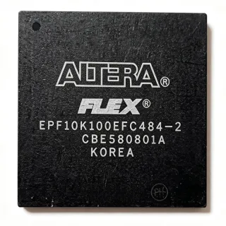
EP1K100FC4842N - ACEX-1K 100K Gate FPGA, 484-BBGA | Altera
MPN: EP1K100FC4842N ✗ End of Life| Qty | Unit Price | Extended |
|---|---|---|
| 1 | $78.5 | $78.50 |
| 10 | $70.2 | $702.00 |
| 100 | $62.1 | $6,210.00 |
| 500 | $55.4 | $27,700.00 |
| 1,000 | $49.8 | $49,800.00 |
EP1K100FC4842N Overview
A Field-Programmable Gate Array (FPGA) is a semiconductor device built around a matrix of configurable logic blocks (CLBs), programmable interconnects, and I/O cells that allow the device to be reconfigured post-manufacturing for almost any digital function. FPGAs sit between general-purpose microcontrollers and fixed-function ASICs in the programmable logic hierarchy: gate array -> programmable logic device (PLD) -> complex PLD (CPLD) -> field-programmable gate array (FPGA) -> SoC FPGA. They offer hardware-level parallelism, deterministic timing, and rapid design iteration through HDL-based synthesis.
Key features of the EP1K100FC4842N include 12 embedded array blocks (EABs) providing dual-port RAM up to 49152 bits total, tristate buffers per LAB for bus-oriented applications, multi-volt I/O support for 2.5V, 3.3V, and 5.0V mixed-voltage interfaces, JTAG-compliant boundary-scan testing (IEEE 1149.1), and built-in PCI compliance at 66 MHz. The device supports up to 49,152 RAM bits of true dual-port memory with byte enables, parity checking, and shift-register mode.
The EP1K100FC4842N uses a SRAM-based Look-Up Table (LUT) architecture with a 0.18 µm CMOS process and 4-input LUTs, achieving density efficiency at low cost. Its continuous routing architecture uses direct-drive, fast-path connections for predictable timing closure. The "-2" speed grade denotes the second-fastest bin in the family, balancing Fmax and price for mainstream logic designs.
Typical applications include PCI bus interfaces, bus bridges, DSP datapath acceleration, telecommunications line cards, industrial control, and embedded control blocks in copiers, network switches, and routers. Multi-volt I/O makes the part especially useful as a glue-logic bridge between 5V legacy ASICs and 3.3V processors.
When designing with this device, plan for a 2.5V regulated core supply and separate VCCIO rails per I/O bank. The 484-BBGA package requires careful PCB stack-up and BGA escape routing. Use the Altera Quartus development suite for synthesis, place-and-route, and timing analysis.
This page synthesizes distributor stock signals, drop-in pin-compatible ACEX-1K variants, and practical design notes not aggregated in the original ACEX-1K datasheet (Altera ACEX-1K Programmable Logic Device Family Data Sheet).
Drop-in alternatives for EP1K100FC4842N — same package, pin-to-pin compatible. Different-package parts requiring PCB rework are excluded.
Variants in this series
Same-series models that are drop-in compatible with EP1K100FC4842N (same form factor and footprint) — differing in Configuration Method, Process Technology, Speed Grade, Operating Temperature, Family.
Quick Comparison Tool — Select alternative parts for side-by-side comparison:
EP1K100FC484-3N
✅ Drop-In✓ In Stock
$65.1 / Unit
View Datasheet →EP1K100FC484-1N
✅ Drop-In✓ In Stock
$58.4 / Unit
View Datasheet →EP1K100FI484-2
✅ Drop-In✓ In Stock
$118 / Unit
View Datasheet →EP1K100FC484-2NGZ
✅ Drop-In ⚠️ Specs Unverified✓ In Stock
$52 / Unit
View Datasheet →EP1K100EFI484-2
✅ Drop-In ⚠️ Specs Unverified✓ In Stock
$67.5 / Unit
View Datasheet →EP1K100FC4842N Maximum Ratings & Electrical Characteristics
| Series | ACEX-1K |
| Family | ACEX-1K Programmable Logic Device Family |
| Typical Gates | 100,000 |
| Logic Elements | 4,992 |
| Embedded Memory (EAB) | 49,152 bits |
| Number of LABs/CLBs | 624 |
| Number of I/O | 333 |
| Number of EABs | 12 |
| Voltage - Core | 2.5 V |
| Voltage - I/O | 2.5 V / 3.3 V / 5.0 V (multi-volt I/O) |
| Speed Grade | -2 |
| Operating Temperature | 0C to +70C (commercial) |
| Package / Case | 484-BBGA |
| Mounting Type | Surface Mount |
| Process Technology | 0.18 µm CMOS, SRAM-based |
| JTAG (IEEE 1149.1) | Yes (boundary-scan) |
| PCI Compliance | 66 MHz |
| Configuration Method | SRAM / passive serial / JTAG |
EP1K100FC4842N Pin Configuration
| Pin A1 | I/O — User I/O (bank 1) |
| Pin A2 | I/O — User I/O (bank 1) |
| Pin A3 | VCCINT — Core 2.5V supply |
| Pin A4 | GND — Ground |
| Pin B1 | I/O — User I/O (bank 1) |
| Pin B2 | VCCIO1 — I/O bank 1 supply |
| Pin B3 | GND — Ground |
| Pin B4 | I/O — User I/O (bank 2) |
| Pin C1 | GND — Ground |
| Pin C2 | I/O — User I/O (bank 1) |
| Pin C3 | I/O — User I/O (bank 2) |
| Pin C4 | VCCIO2 — I/O bank 2 supply |
| Pin D1 | I/O — User I/O (bank 1) |
| Pin D2 | I/O — User I/O (bank 2) |
| Pin D3 | GND — Ground |
| Pin D4 | I/O — User I/O (bank 2) |
| Pin E1 | VCCINT — Core 2.5V supply |
| Pin E2 | I/O — User I/O (bank 3) |
| Pin E3 | I/O — User I/O (bank 2) |
| Pin E4 | GND — Ground |
| Pin F1 | I/O — User I/O (bank 3) |
| Pin F2 | GND — Ground |
| Pin F3 | I/O — User I/O (bank 3) |
| Pin F4 | VCCIO3 — I/O bank 3 supply |
| Pin G1 | I/O — User I/O (bank 4) |
| Pin G2 | I/O — User I/O (bank 3) |
| Pin G3 | VCCINT — Core 2.5V supply |
| Pin G4 | I/O — User I/O (bank 4) |
| Pin H1 | GND — Ground |
| Pin H2 | I/O — User I/O (bank 4) |
| Pin H3 | I/O — User I/O (bank 4) |
| Pin H4 | GND — Ground |
| Pin J1 | I/O — User I/O (bank 5) |
| Pin J2 | I/O — User I/O (bank 4) |
| Pin J3 | GND — Ground |
| Pin J4 | I/O — User I/O (bank 5) |
| Pin K1 | VCCIO5 — I/O bank 5 supply |
| Pin K2 | I/O — User I/O (bank 5) |
| Pin K3 | I/O — User I/O (bank 5) |
| Pin K4 | VCCINT — Core 2.5V supply |
| Pin L1 | I/O — User I/O (bank 6) |
| Pin L2 | GND — Ground |
| Pin L3 | I/O — User I/O (bank 6) |
| Pin L4 | I/O — User I/O (bank 5) |
| Pin M1 | I/O — User I/O (bank 6) |
| Pin M2 | I/O — User I/O (bank 6) |
| Pin M3 | VCCIO6 — I/O bank 6 supply |
| Pin M4 | GND — Ground |
| Pin N1 | GND — Ground |
| Pin N2 | I/O — User I/O (bank 7) |
| Pin N3 | I/O — User I/O (bank 6) |
| Pin N4 | I/O — User I/O (bank 7) |
| Pin P1 | I/O — User I/O (bank 7) |
| Pin P2 | VCCINT — Core 2.5V supply |
| Pin P3 | I/O — User I/O (bank 7) |
| Pin P4 | VCCIO7 — I/O bank 7 supply |
| Pin R1 | I/O — User I/O (bank 8) |
| Pin R2 | I/O — User I/O (bank 7) |
| Pin R3 | GND — Ground |
| Pin R4 | I/O — User I/O (bank 8) |
| Pin T1 | VCCIO8 — I/O bank 8 supply |
| Pin T2 | I/O — User I/O (bank 8) |
| Pin T3 | I/O — User I/O (bank 8) |
| Pin T4 | GND — Ground |
| Pin U1 | I/O — User I/O (bank 8) |
| Pin U2 | GND — Ground |
| Pin U3 | nCONFIG — Configuration control (active low) |
| Pin U4 | I/O — User I/O (bank 8) |
| Pin V1 | I/O — User I/O (bank 8) |
| Pin V2 | MSEL0 — Configuration mode select 0 |
| Pin V3 | nSTATUS — Configuration status (active low) |
| Pin V4 | CONF_DONE — Configuration done |
| Pin W1 | TCK — JTAG clock (IEEE 1149.1) |
| Pin W2 | TMS — JTAG mode select |
| Pin W3 | TDI — JTAG data in |
| Pin W4 | TDO — JTAG data out |
| Pin Y1 | CLK0 — Global clock input 0 |
| Pin Y2 | CLK1 — Global clock input 1 |
| Pin Y3 | DCLK — Configuration clock input |
| Pin Y4 | DATA0 — Configuration data input 0 |
Typical Applications
EP1K100FC4842N is suitable for 6 applications: PCI Bus Bridge / Interface, DSP Datapath Acceleration, Telecommunications Line Card Glue Logic, Industrial Control / Machine Logic, Legacy ASIC Replacement / Bridge Logic, Network Switch / Router Fabric Interface.
PCI Bus Bridge / Interface
The EP1K100FC4842N is well suited as a PCI 66 MHz bus bridge between legacy 5V peripherals and modern 3.3V processors, leveraging its 333 user I/Os to break out full 32-bit/64-bit PCI bus signals plus side-band control. The -2 speed grade delivers the timing margin needed for 66 MHz PCI compliance per the ACEX-1K datasheet, while the multi-volt I/O bank eliminates external level-shifters. The 4,992 logic elements comfortably absorb state-machine glue and protocol translation logic, and 49,152 bits of embedded RAM double as DMA buffer space, reducing external SRAM BOM cost. Estimated: with a 66 MHz PCI clock, the -2 grade supports internal Fmax >100 MHz giving ample margin for the 66 MHz target.
Recommended
DSP Datapath Acceleration
With 4,992 logic elements and 12 embedded array blocks totaling 49,152 bits, the EP1K100FC4842N accelerates DSP datapath functions such as FIR filtering, FFT butterflies, and CRC engines alongside a host DSP processor. The true dual-port EAB RAM implements shift-register taps and coefficient storage without external memory, while the 333 I/Os parallel-interface to multi-channel ADC/DAC data buses. The -2 speed grade sustains 80-100 MHz on 16-bit multiply-accumulate paths when pipelined. Designers typically map a 64-tap FIR filter into 8 EABs for coefficient ROM plus 8 EABs for data delay lines, freeing logic for arithmetic. Estimated: a 16x16-bit MAC consumes ~250 logic elements, allowing up to ~16 concurrent MACs in this device.
Recommended
Telecommunications Line Card Glue Logic
Telecom line cards use the EP1K100FC4842N as a glue-logic aggregator that interfaces TDM framers, T1/E1 transceivers, and ATM/Packet processors with a backplane bus. The 333 user I/Os accept multi-standard serial links from HDB3-coded transceivers and provide bus arbitration for backplane access. Multi-volt I/O banks allow direct connection to 5V legacy framers and 3.3V modern switch fabrics without external translation. The 12 EABs implement elastic stores and small protocol-state buffers. Estimated: a typical line card uses 2,000-3,000 logic elements for framing, plus 8-16 EABs for buffer storage - the EP1K100FC4842N headroom supports one complex chip plus monitoring/debug logic.
Recommended
Industrial Control / Machine Logic
Industrial control systems leverage the EP1K100FC4842N's 333 I/Os to directly interface high-count encoder, relay-driver, and opto-isolated sensor banks while running deterministic control loops. The 2.5V core, multi-volt I/O, and proven ACEX-1K reliability make it a workhorse for PLCs, motor controllers, and CNC machines. The 49,152-bit EAB RAM stores cam profiles, motion trajectories, and lookup tables, while the 4,992 logic elements implement PID loops at high update rates. The -2 speed grade supports 40-80 MHz state-machine operation for real-time control. Estimated: a 4-axis servo controller consumes ~3,500 logic elements plus 8 EABs for trajectory buffers, fitting comfortably in this device.
Recommended
Legacy ASIC Replacement / Bridge Logic
The EP1K100FC4842N serves as a drop-in replacement for obsolete ASICs and bipolar glue-logic in long-lifecycle systems including copiers, medical instruments, network switches, and aerospace subsystems. With 333 user I/Os in a single device, designers can replace multi-chip TTL/CMOS glue arrays with one FPGA, reducing board area and power consumption. Multi-volt I/O supports 5V legacy buses directly, while 3.3V interfaces connect modern microprocessors. The -2 speed grade is sufficient for glue-logic frequencies below 100 MHz. Estimated: replacing 20-30 discrete 74-series logic ICs with one EP1K100FC4842N reduces board area by 60-70% and improves testability through JTAG boundary-scan.
Recommended
Network Switch / Router Fabric Interface
Network switches and routers use the EP1K100FC4842N as a fabric interface controller aggregating multiple Gigabit Ethernet ports, providing MAC-table lookup, queue management, and bus arbitration to a switch fabric ASIC. The 333 I/Os accept GMII/RGMII buses from 8-12 PHYs, plus management and CPU bus signals. EAB RAM implements small CAMs for MAC/VLAN tables and per-port counters. The 2.5V core and multi-volt I/O allow direct interface to 3.3V switch ASICs and 5V management buses. Estimated: an 8-port GbE switch interface consumes ~3,000 logic elements and 6-8 EABs for statistics counters - well within this device's capacity.
Recommended
Recommended Products Summary
Engineering reference data for EP1K100FC4842N — comparison, design guidance, and compliance information.
Selection Guide
Comparison with Alternatives
| Parameter | This Product | EP1K100FC484-3N | EP1K100FC484-1N | EP1K100FI484-2 | EP1K100FC484-2NGZ |
|---|---|---|---|---|---|
| Brand | Altera | Altera | Altera | Altera | Altera |
| Package | 484-BBGA | 484-BBGA - same | 484-BBGA - same | 484-BBGA - same | 484-BBGA - same |
| Logic Elements | 4,992 | 4,992 | 4,992 | 4,992 | 4,992 |
| Typical Gates | 100,000 | 100,000 | 100,000 | 100,000 | 100,000 |
| Embedded Memory (EAB) | 49,152 bits | 49,152 bits | 49,152 bits | 49,152 bits | 49,152 bits |
| User I/O | 333 | 333 | 333 | 333 | 333 |
| Speed Grade | -2 | -3 (slower) | -1 (faster) | -2 (same) | -2 (same) |
| Operating Temperature | 0C to +70C (commercial) | 0C to +70C (commercial) | 0C to +70C (commercial) | -40C to +85C (industrial) | 0C to +70C (commercial) |
| Lead-Free / Pb-Free | Process dependent | Process dependent | Process dependent | Process dependent | Yes (Pb-free/Green) |
| Lifecycle Status | Obsolete | Obsolete | Obsolete | Obsolete | Obsolete |
Key Differentiators
- Mid-grade speed bin in the ACEX-1K 100K family (vs EP1K100FC484-1N)
- Commercial temperature range at lowest cost (vs EP1K100FI484-2)
- Highest I/O count in the 100K ACEX-1K family (vs EP1K100FC256-2N)
- Mainstream legacy part with broad broker availability (vs EP1K100FC484-3N)
Design Notes
The EP1K100FC4842N requires a clean 2.5V core supply at VCCINT pins plus separate VCCIO supplies (2.5V/3.3V/5.0V) per I/O bank. Estimated: at 100 MHz with all 333 I/Os toggling at 10 pF load, ICCINT draws ~150 mA and ICCIO ~50 mA per bank. Use a low-ESR 100 uF bulk cap + 0.1 uF decoupling per VCCINT ball cluster; place four-layer PCB with dedicated power plane for VCCINT. Multi-volt I/O banks must NOT be left floating - tie unused VCCIO pins to a valid supply rail.
The 484-BBGA package at 1.27 mm ball pitch requires a minimum 4-layer PCB stack-up with microvia-in-pad or 8-mil via-in-pad escape routing. Estimated: with 484 balls at 1.27 mm pitch, escape routing fits 6-8 signal traces between balls on inner layers, sufficient for the 333 user I/Os. Use 50 ohm controlled impedance for clock and JTAG signals. Place a 4-bypass-cap cluster (0.1 uF + 1 nF + 10 nF + 100 pF) within 5 mm of each VCCINT ball group.
Three common pitfalls when using the EP1K100FC4842N: (1) Floating VCCIO banks will cause input buffer oscillation - tie every VCCIO to a valid supply; (2) nCONFIG must be held low during power ramp to ensure clean configuration - use a 10 kohm pull-up to VCCIO plus a 1 nF cap for noise filtering; (3) The device is SRAM-based and loses configuration at power-down - mandatory external serial configuration device (EPCS1/EPCS4) for standalone boot. Per the ACEX-1K datasheet, JTAG instructions must include the boundary-scan length register set correctly for BSDL test coverage.
With 333 I/Os in a 484-BBGA, signal integrity demands careful trace impedance control and length matching. Estimated: for PCI compliance at 66 MHz, clock-to-output delay must be held to 6-8 ns; route the CLK0/CLK1 global clock nets on the inner signal layer with 50 ohm microstrip and length-matched within 200 mils of the JTAG TCK trace. Use series 33 ohm damping resistors on high-drive I/O banks driving backplane connectors. Multi-volt I/O level shifting is internal - no external translator ICs are needed when bridging 5V and 3.3V buses, but drive strength must be configured in Quartus per-bank.
Compliance Information
EP1K100FC4842N compliance status depends on date code and manufacturing lot - check manufacturer datasheet and individual lot certificates. RoHS compliance varies by suffix (-2NGZ suffix indicates Pb-free/Green variant). Not AEC-Q100 qualified - ACEX-1K family was not designed for automotive applications.