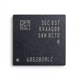
H5ANAG8NCMR-XNI - 16Gb DDR4 SDRAM 3200Mbps | SK Hynix
MPN: H5ANAG8NCMR-XNI ✓ Active| Qty | Unit Price | Extended |
|---|---|---|
| 1 | $5.9 | $5.90 |
| 10 | $5.45 | $54.50 |
| 100 | $4.95 | $495.00 |
| 500 | $4.55 | $2,275.00 |
| 1,000 | $4.15 | $4,150.00 |
H5ANAG8NCMR-XNI Overview
DRAM (Dynamic Random Access Memory) is a type of volatile semiconductor memory that stores each bit in a separate capacitor within an integrated circuit. In the memory hierarchy, DDR4 SDRAM sits as the main-system-memory technology between cache (SRAM) and storage (NAND flash), and the H5ANAG8NCMR-XNI is a component-level DRAM die packaged as a discrete IC intended for solder-down or DIMM-module use in large-density main memory applications.
Key features include the 16Gb single-die density, an x8 organization, and 3200Mbps data rate per pin, which corresponds to DDR4-3200 operation. The -XNI speed grade and lead-finish suffix code identify operating speed and environmental compliance per SK Hynix ordering-code conventions. The 78-ball FBGA surface-mount package minimizes signal-path length, supporting the high-speed switching margins required at DDR4 frequencies.
Technically, this device is a CMOS DDR4 SDRAM implementing the JEDEC DDR4 interface: 1.2V operation, differential clocking, bank-group architecture, and on-die termination. These features reduce I/O power and allow multiple chip-selects to share a common bus with controlled stub length. As a volatile memory format (DRAM), it requires periodic refresh, which the internal controller handles automatically per the DDR4 protocol.
Typical applications include desktop and notebook DIMM modules, server RDIMM/LRDIMM main memory, embedded systems requiring high-density RAM, networking equipment buffers, and industrial computing platforms where large memory density and high bandwidth are required.
A key design consideration is signal integrity: at 3200Mbps, fly-by routing, controlled impedance, and VTT termination must follow the manufacturer datasheet layout guidance. Confirm the exact speed grade and module-load conditions against the official SK Hynix datasheet before finalizing memory-controller timing parameters.
This page synthesizes distributor stock and pricing data, drop-in alternatives, and practical design notes not found in the manufacturer datasheet.
Drop-in alternatives for H5ANAG8NCMR-XNI — same package, pin-to-pin compatible. Different-package parts requiring PCB rework are excluded.
Variants in this series
Same-series models that are drop-in compatible with H5ANAG8NCMR-XNI (same form factor and footprint) — differing in Package, Data Rate, Memory Type, Memory Organization, RoHS Status.
Quick Comparison Tool — Select alternative parts for side-by-side comparison:
H5ANAG8NCJR-XNC
✅ Drop-In✓ In Stock
$65.625 / Unit
View Datasheet →H5ANAG8NCMR-VKC
✅ Drop-In✓ In Stock
$8.05 / Unit
View Datasheet →H5ANAG8NAMR-UHC
✅ Drop-In✓ In Stock
$2.15 / Unit
View Datasheet →H5ANAG8NCMR-XNC
✅ Drop-In📋 Reference alternative (not in catalog)
H5ANAG8NBJR-PBC
✅ Drop-In✓ In Stock
$31.5 / Unit
View Datasheet →MT40A2G8AG-062E
✅ Drop-In✓ In Stock
$9.75 / Unit
View Datasheet →H5ANAG8NCMR-XNI Maximum Ratings & Electrical Characteristics
| Memory Type | Volatile (DRAM) |
| Memory Format | DDR4 SDRAM |
| Memory Size | 16 Gb |
| Memory Organization | x8 |
| Interface | Parallel |
| Data Rate | 3200 Mbps (DDR4-3200) |
| Supply Voltage (VDD) | 1.2 V |
| Package | FBGA-78 |
| Mounting Type | Surface Mount |
| Packaging | Tray |
| Product Status | Active |
| Manufacturer | SK Hynix |
| Technology | CMOS DDR4 SDRAM |
H5ANAG8NCMR-XNI fbga-78 Pin Configuration Guide
Pin configuration for H5ANAG8NCMR-XNI (fbga-78 package). This digital IC includes GPIO, communication interfaces (UART, SPI, I2C), and power pins. Refer to the manufacturer datasheet for alternate pin functions and configuration options. Essential for embedded system design and PCB layout.

No detailed pinout data available for H5ANAG8NCMR-XNI.
Refer to the datasheet for full pin configuration.
Typical Applications
H5ANAG8NCMR-XNI is suitable for 6 applications: Server RDIMM Main Memory, Desktop and Notebook DIMM Modules, Networking and Communication Equipment, Embedded and Industrial Computing, Graphics and Display Buffer Memory, Test and Measurement Instrumentation.
Server RDIMM Main Memory
In server memory subsystems, the H5ANAG8NCMR-XNI provides 16Gb per device at 3200Mbps, enabling high-capacity RDIMM and LRDIMM modules where aggregate bandwidth is the primary performance metric. Its x8 organization allows error-correction schemes (chipkill/single-device data correction) on x8 DRAM devices, which server platforms require for data integrity. Placed on a fly-by-routed DIMM command/address bus with on-die termination (ODT) and VTT termination, the device sustains DDR4-3200 signaling while minimizing stub reflections. Designers should budget for refresh overhead and validate RCD (registering clock driver) compatibility, typically pairing with register ICs supporting DDR4-3200 data rates.
Recommended
Desktop and Notebook DIMM Modules
Consumer and commercial PC DIMMs use 16Gb x8 DDR4 components such as the H5ANAG8NCMR-XNI to reach 16GB and 32GB per module at DDR4-3200. The 1.2V supply keeps module power within JEDEC DDR4 budgets, and the 78-ball FBGA package supports standard x8 chip layouts on 288-pin UDIMM/SO-DIMM land patterns. Because the part is pin-compatible within the SK Hynix 16Gb x8 family, module makers can dual-source between speed-grade suffixes without PCB changes. Key design items include DQS strobe fly-by termination, ZQ calibration resistor placement, and temperature-compensated refresh configuration for consumer operating ranges.
Recommended
Networking and Communication Equipment
Routers, switches, and telecom line cards buffer packet data in large DRAM arrays; the H5ANAG8NCMR-XNI's 16Gb density and 3200Mbps bandwidth support high-throughput queue and flow tables. In solder-down configurations, four to eight devices on a 64-bit bus deliver 25.6 GB/s theoretical bandwidth per channel at DDR4-3200. The DDR4 bank-group architecture reduces effective access latency for the bursty random traffic typical of packet buffering. Designers must control trace-length skew within datasheet limits and verify VREFCA/VREFDQ tolerance under the equipment's thermal envelope to maintain margin at full data rate.
Recommended
Embedded and Industrial Computing
Industrial PCs, gateways, and machine-vision controllers use solder-down DDR4 like the H5ANAG8NCMR-XNI for 8-32GB main memory in conduction-cooled enclosures. The 1.2V operation reduces heat dissipation versus DDR3 (1.5V), which matters in sealed, fanless systems; a single 16Gb x8 device can serve half of a 64-bit channel, simplifying BOM for 4GB-8GB designs. Industrial programs benefit from the part's active lifecycle status and cross-vendor drop-in availability (Micron MT40A2G8AG-062E). Memory-controller training and margin testing should be executed at the worst-case industrial temperature to guarantee timing closure at 3200Mbps.
Recommended
Graphics and Display Buffer Memory
Smart displays, digital signage players, and set-top SoC platforms use 16Gb x8 DDR4 such as the H5ANAG8NCMR-XNI as frame buffer and application memory. At 3200Mbps, one x8 device provides 3.2 GB/s per channel segment, enough for 4K30 decode plus UI compositing when combined in 32-bit or 64-bit buses. The on-die termination and 1.2V I/O reduce EMI - an important consideration in consumer AV equipment passing CISPR-class radiated emission limits. Layout should keep DQ/DQS length matching within datasheet skew specs and place the ZQ calibration resistor with a clean ground reference for stable output impedance.
Recommended
Test and Measurement Instrumentation
Oscilloscopes, logic analyzers, and protocol analyzers require deep capture memory; arrays of 16Gb DDR4 devices like the H5ANAG8NCMR-XNI provide multi-gigabyte record lengths. Its 3200Mbps rate sustains streaming acquisition data into memory, while the x8 organization supports ECC-protected acquisition buffers on 72-bit buses (64 data + 8 check bits per 9 devices). Instrument makers value the strong multi-distributor stock (36,000+ pcs in August 2026) for production continuity. Design effort centers on power delivery: per-device peak current during burst writes requires local decoupling and careful VDDQ plane segmentation to avoid droop-induced eye collapse.
Recommended
Recommended Products Summary
Engineering reference data for H5ANAG8NCMR-XNI — comparison, design guidance, and compliance information.
Selection Guide
Comparison with Alternatives
| Parameter | This Product | H5ANAG8NCJR-XNC | H5ANAG8NCMR-VKC | H5ANAG8NAMR-UHC | MT40A2G8AG-062E |
|---|---|---|---|---|---|
| Package | FBGA-78 | FBGA-78 - same | FBGA-78 - same | FBGA-78 - same | FBGA-78 - same |
| Brand | SK Hynix | SK Hynix | SK Hynix | SK Hynix | Micron Technology |
| Memory Size | 16 Gb | 16 Gb | 16 Gb | 16 Gb | 16 Gb |
| Organization | x8 | x8 | x8 | x8 | x8 |
| Memory Technology | DDR4 SDRAM | DDR4 SDRAM | DDR4 SDRAM | DDR4 SDRAM | DDR4 SDRAM |
| Supply Voltage | 1.2 V | 1.2 V | 1.2 V | 1.2 V | 1.2 V |
| Packaging | Tray | Tray | Tray | Tray | Tray |
| Product Status | Active | Active | Active | Active | Active |
Key Differentiators
- Highest speed grade in the 16Gb x8 DDR4 family (vs H5ANAG8NCJR-XNC)
- 16Gb single-device density maximizes capacity per chip-select (vs H5AN8G8NCJR-XNC)
- Cross-brand second-source availability (vs MT40A2G8AG-062E)
Design Notes
At 3200Mbps, DDR4 signal integrity dominates design success. Use fly-by routing for command/address with series termination to VTT; keep DQ/DQS length matching within datasheet skew limits and maintain controlled impedance (40 ohm single-ended, 80 ohm differential for DQS pairs). Read/write eye margin must be validated with the memory controller's training algorithms at worst-case temperature. Estimated: a 64-bit bus of eight x8 devices at 3200Mbps yields 25.6 GB/s theoretical bandwidth; verify actual efficiency (typically 60-70%) for your access pattern.
VDD and VDDQ are nominally 1.2V for DDR4. Estimate per-device peak current during full-burst writes: with DQ current on the order of hundreds of milliamps per device during toggling, eight devices on one channel can demand several amps transient current. Provide local bulk plus high-frequency ceramic decoupling at each device and a low-inductance VDDQ plane. Note this is an estimate - consult the SK Hynix datasheet IDD specification tables for exact current figures before finalizing the power tree.
Speed-grade suffixes matter: substituting a -XNC (lower grade) into a DDR4-3200 design will fail initialization or margin testing, while using this -XNI part at a lower configured grade is safe. Always decode the full ordering code (die revision, speed, lead finish) from the SK Hynix datasheet ordering-information table before approving second sources, and re-run controller read/write training and DRAM margin tests after any vendor or suffix change.
Compliance Information
Compliance status not stated in the provided web data; confirm RoHS/REACH status via the SK Hynix official environmental datasheet. The -XNI suffix may encode lead-finish information per SK Hynix ordering conventions - verify in the datasheet.