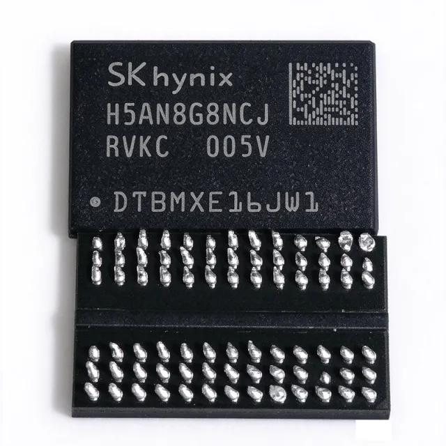
H5ANAG8NCJR-XNC - 16Gb DDR4-3200 SDRAM 2Gx8 | SK Hynix
MPN: H5ANAG8NCJR-XNC ✓ Active| Qty | Unit Price | Extended |
|---|---|---|
| 1 | $112.5 | $112.50 |
| 10 | $81.25 | $812.50 |
| 100 | $71.875 | $7,187.50 |
| 500 | $68.75 | $34,375.00 |
| 1,000 | $65.625 | $65,625.00 |
H5ANAG8NCJR-XNC Overview
A DDR4 SDRAM (Double Data Rate Fourth Generation Synchronous Dynamic Random Access Memory) is the mainstream volatile main-memory technology for computing systems. In the memory hierarchy, DRAM sits between CPU caches (SRAM) and persistent storage (NAND flash / SSDs), providing high-bandwidth working memory. DDR4 doubled the internal bank count of DDR3 (16 banks in 4 bank groups) and lowered the I/O voltage from 1.5 V to 1.2 V, improving bandwidth per watt. A DRAM controller inside the host SoC or memory controller manages refresh, bank interleaving, and DDR4 protocol timing, so this chip is never used standalone - it is soldered to a memory bus alongside a processor, FPGA with hard memory controller, or memory-companion chip.
Key features include 16 Gbit density per monolithic die, an x8 organization (2G addressable words x 8 bits), and DDR4-3200 operation (3200 MT/s), yielding up to 25.6 GB/s of peak bandwidth per 64-bit channel when populated 8-deep. The XNC speed grade is specified over 0C to +95C. Per TechInsights teardown analysis, the H5ANAG8NCJR-XNC contains the H5ANAG6NC die, SK hynix's first 1z nm node DRAM, offering the smallest 16Gb DDR4 die size and highest bit density (0.296 Gb/mm2) of its generation, built on non-EUV lithography.
Architecturally, DDR4 devices use a multi-bank-group array with bank-group-wise row activation, a DLL for output timing, and on-die VDDQ termination (ODT) to preserve signal integrity at 3200 MT/s. The 1z nm process shrinks the cell transistor and capacitor, reducing standby and active current versus earlier 1x/1y nm parts.
Typical applications include industrial controllers and computing modules requiring large memory density, firmware boot and embedded logging buffers, SSD controller write caches, and replacement sourcing for DDR4-based main memory on servers, workstations, and networking line cards.
Design consideration: DDR4-3200 routing requires length-matched fly-by termination and careful DQS/DQ skew budgeting; always tie CA parity and alert pins per the JEDEC DDR4 convention and your memory controller's compatibility guide.
This page synthesizes distributor pricing and stock, drop-in same-family alternatives, and practical design notes not found in the manufacturer datasheet.
Drop-in alternatives for H5ANAG8NCJR-XNC — same package, pin-to-pin compatible. Different-package parts requiring PCB rework are excluded.
Variants in this series
Same-series models that are drop-in compatible with H5ANAG8NCJR-XNC (same form factor and footprint) — differing in Package, Data Rate, Interface, Organization, RoHS Status.
Quick Comparison Tool — Select alternative parts for side-by-side comparison:
H5ANAG8NBJR-VKC
✓ In Stock
$8.6 / Unit
View Datasheet →H5ANAG8NBJR-RDC
✓ In Stock
$3.55 / Unit
View Datasheet →H5ANAG8NBJR-PBC
✓ In Stock
$31.5 / Unit
View Datasheet →H5AN8G8NCJR-XNC
✓ In Stock
$30.6923 / Unit
View Datasheet →H5ANAG8NCJR-XNC Maximum Ratings & Electrical Characteristics
| Memory Type | DDR4 SDRAM |
| Density | 16 Gbit |
| Organization | 2G x 8 |
| Data Rate | 3200 MT/s (DDR4-3200) |
| Supply Voltage (VDD) | 1.2 V |
| Package | FBGA-78 (7.5 x 11 mm) |
| Operating Temperature | 0C to +95C |
| Mounting Type | Surface Mount |
| Process Node | 1z nm (non-EUV) |
| Die Bit Density | 0.296 Gb/mm2 |
| Peak Bandwidth (per 64-bit channel) | 25.6 GB/s at DDR4-3200 |
| RoHS Status | Compliant |
| Base Part Number Family | H5ANAG8NCJR (16Gb DDR4 CMOS SDRAM) |
| Speed Grade Suffix | -XNC (0~95C commercial) |
H5ANAG8NCJR-XNC fbga-78 (7.5 x 11 mm) Pin Configuration Guide
Pin configuration for H5ANAG8NCJR-XNC (fbga-78 (7.5 x 11 mm) package). This digital IC includes GPIO, communication interfaces (UART, SPI, I2C), and power pins. Refer to the manufacturer datasheet for alternate pin functions and configuration options. Essential for embedded system design and PCB layout.

No detailed pinout data available for H5ANAG8NCJR-XNC.
Refer to the datasheet for full pin configuration.
Typical Applications
H5ANAG8NCJR-XNC is suitable for 6 applications: Industrial Computing Modules, Server and Workstation Main Memory, SSD Controller Write Cache, FPGA-Based Data Acquisition and Logging, Networking Line Cards, DDR4 Replacement Sourcing and Repair.
Industrial Computing Modules
The H5ANAG8NCJR-XNC fits industrial computing modules and embedded controllers that need main memory density without DIMM sockets. Its 16Gb monolithic die in a 7.5 x 11 mm FBGA-78 delivers 2 GB per x8 device, so a 64-bit channel of eight devices reaches 16 GB while conserving board area on COM Express or SMARC carriers. DDR4-3200 operation supplies up to 25.6 GB/s per channel, sufficient for industrial vision, motion control, and protocol processing. The 0C to +95C rating covers typical enclosed industrial environments; design for the 1.2 V rail with ODT tuning per the memory controller's compatibility guide, and qualify same-family NBJR alternates for supply-chain resilience.
Recommended
Server and Workstation Main Memory
In server DIMM and memory-down designs, the H5ANAG8NCJR-XNC provides 16Gb DDR4-3200 devices for high-bandwidth main memory. A 64-bit rank of eight devices achieves 16 GB per rank at 25.6 GB/s peak bandwidth; multi-rank boards stack chip-selects for capacity scaling. The 1z nm die's 0.296 Gb/mm2 density lowers per-bit power versus 1x/1y nm predecessors, helping TDM (thermal design margins) in dense 1U servers. DDR4's bank-group architecture sustains 3200 MT/s with fly-by termination, but PCB designers must length-match DQ byte lanes within +/-25 mil class rules and follow the controller's write-leveling procedure.
Recommended
SSD Controller Write Cache
Enterprise and industrial SSD controllers use DDR4 DRAM as mapping-table (FTL) memory and write cache. The H5ANAG8NCJR-XNC's 2 GB per device supports large-capacity NVMe drives with multi-terabyte LBA maps, while DDR4-3200 bandwidth keeps random-write latency low. Because the FBGA-78 footprint is identical across SK hynix 8Gb/16Gb x8 family members, a single PCB layout can be populated for 4 GB (two devices) or 8 GB (four devices) cache tiers, simplifying SKU management. Ensure the SSD controller supports DDR4-3200 training, or clock down to a common speed bin; the -XNC part is backward-compatible with lower DDR4 data rates per the JEDEC DDR4 protocol.
Recommended
FPGA-Based Data Acquisition and Logging
High-speed data acquisition systems built on SoC FPGAs use the H5ANAG8NCJR-XNC as streaming buffer memory for embedded logging. A 16Gb x8 device buffers gigabytes of ADC samples between bursts, and DDR4-3200 transfers clear FIFO backlogs at up to 3.2 GB/s per x8 device. Intel Arria 10-class devices (e.g., 10AS032 series) integrate hard DDR4 memory controllers that interface directly with the 1.2 V FBGA-78 device. Design attention should focus on address/command fly-by topology, ODT calibration during memory training, and refresh-borrow-aware buffering so refresh cycles do not overflow capture FIFOs at maximum sustained sample rates.
Recommended
Networking Line Cards
Switch, router, and firewall line cards employ DDR4 for packet buffering, flow tables, and deep-packet-inspection state. The H5ANAG8NCJR-XNC's 2 GB density per FBGA-78 device lets designers populate 8-16 GB per card without high-layer-count memory buses, and the 1z nm process reduces standby current for always-on networking equipment. DDR4-3200 supports line-rate small-packet forwarding when paired with efficient QoS schedulers. Thermal design matters in 1U chassis: with limited airflow, derate the junction temperature using the family datasheet thermal resistance data and consider spread-spectrum clocking to manage EMI on high-speed DQ buses.
Recommended
DDR4 Replacement Sourcing and Repair
For board-level repair, replacement sourcing, and shortage mitigation, the H5ANAG8NCJR-XNC serves as a direct-fit 16Gb DDR4-3200 x8 component for memory-down PCBs originally built with SK hynix FBGA-78 DDR4. Buyers should match the exact suffix (-XNC, 0-95C, DDR4-3200) where timing tables are controller-qualified, or qualify NBJR-family alternates from the same footprint for second-sourcing. The 2026 DRAM market has tightened DDR4 supply as HBM capacity expands, so replacement buyers are advised to hold buffer stock and register with multiple distributors for allocation alerts rather than sourcing single-lot spot buys.
Recommended
Recommended Products Summary
Engineering reference data for H5ANAG8NCJR-XNC — comparison, design guidance, and compliance information.
Selection Guide
Comparison with Alternatives
| Parameter | This Product | H5ANAG8NBJR-VKC | H5ANAG8NBJR-RDC | H5ANAG8NBJR-PBC | H5AN8G8NCJR-XNC |
|---|---|---|---|---|---|
| Package | FBGA-78 (7.5 x 11 mm) | FBGA-78 (7.5 x 11 mm) - same | FBGA-78 (7.5 x 11 mm) - same | FBGA-78 (7.5 x 11 mm) - same | FBGA-78 (7.5 x 11 mm) - same |
| Brand | SK Hynix | SK Hynix | SK Hynix | SK Hynix | SK Hynix |
| Density | 16 Gbit | 16 Gbit | 16 Gbit | 16 Gbit | 8 Gbit |
| Organization | 2G x 8 | 2G x 8 | 2G x 8 | 2G x 8 | 1G x 8 |
| Supply Voltage | 1.2 V | 1.2 V | 1.2 V | 1.2 V | 1.2 V |
| RoHS | Compliant | Compliant | Compliant | Compliant | Compliant |
Key Differentiators
- Full 16Gb density per FBGA-78 footprint (vs H5AN8G8NCJR-XNC)
- 1z nm node die (H5ANAG6NC) with 0.296 Gb/mm2 density (vs H5ANAG8NBJR-VKC)
- DDR4-3200 speed class (vs H5ANAG8NBJR-PBC)
Design Notes
At DDR4-3200 (3200 MT/s), signal integrity dominates the design. Use fly-by routing for address/command with per-DIMM/per-rank termination, and length-match DQ byte lanes to their DQS strobes. Set on-die termination (ODT) values during memory training rather than hard-coding, and confirm the host controller's qualified speed bin includes DDR4-3200 for the -XNC grade; otherwise clock down to a common bin.
The device runs from a 1.2 V DDR4 rail with separate VPP and VDDQ domains per the family datasheet. Estimated: at full DDR4-3200 bus utilization with 8 devices on a channel, per-device dissipation is typically on the order of 0.3-0.6 W (exact values depend on read/write mix and refresh rate - consult the datasheet IDD tables for your operating condition). Provide bulk plus per-device 0.1 uF/0.01 uF decoupling close to VDD/VDDQ balls and a solid power plane.
Do not assume all SK hynix FBGA-78 DDR4 suffixes are interchangeable: -XNC denotes DDR4-3200 class over 0C to +95C, while PBC/RDC suffixes may be slower bins. Also beware density confusion - H5AN8G8NCJR (8Gb) shares the footprint with H5ANAG8NCJR (16Gb) but halves capacity. During supply shortage, qualify alternates by datasheet AC timing comparison, not package appearance alone.
Compliance Information
RoHS compliance per JLCPCB part listing. REACH, halogen-free, lead-free, and conflict-minerals declarations not present in provided data - confirm via SK hynix environmental documentation.




