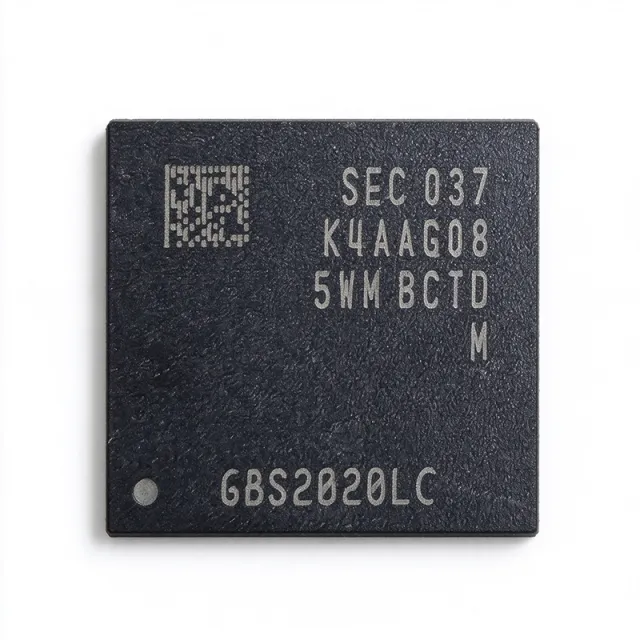
K4AAG085WM-BCTD - 16Gb DDR4-2666 SDRAM, 1.2V | Samsung
MPN: K4AAG085WM-BCTD ✓ Active| Qty | Unit Price | Extended |
|---|---|---|
| 1 | $12.5 | $12.50 |
| 10 | $11.6 | $116.00 |
| 100 | $10.9 | $1,090.00 |
| 500 | $10.4 | $5,200.00 |
| 1,000 | $9.95 | $9,950.00 |
K4AAG085WM-BCTD Overview
DDR4 SDRAM is a type of synchronous DRAM that transfers data on both clock edges (double data rate) and uses a command/address bus with bank-group architecture to achieve high bandwidth. In the memory hierarchy, DDR4 SDRAM sits between embedded SRAM caches and non-volatile storage such as NAND flash, serving as the primary working memory for CPUs, SoCs, and FPGA-based systems.
Key features of the K4AAG085WM-BCTD include a x8 organization (2G addresses x 8 bits), DDR4-2666 speed grade (BCTD bin), low 1.2V core supply for reduced power versus DDR3, and the space-saving FBGA-78 ball grid array package. Samsung part numbering encodes the configuration: K4AAG = 16Gb DDR4, 08 = x8 organization, WM = die/package revision, BCTD = 2666 Mbps speed bin with 0C to +85C operating range.
Architecturally, DDR4 introduces bank groups (up to 4), a lower operating voltage, and a DBI (data bus inversion) capable interface that reduces I/O power. The x8 organization makes the device well suited for ECC-based systems where x8 devices enable single-device data correction (SDDC) on server memory controllers.
Typical applications include industrial controllers, embedded computing modules, data storage appliances, firmware boot buffers, and logging memory in networking and server platforms where 16Gb density and 2666 Mbps bandwidth are required.
Design considerations: DDR4 requires careful signal-integrity work including length-matched fly-by routing of the command/address bus, per-byte termination (ODT) tuning, and VTT termination supply design. Verify controller compatibility for the BCTD timing bin before substitution.
This page synthesizes distributor sourcing data, same-family drop-in alternatives, and practical DDR4 design notes not found in a single manufacturer datasheet.
Drop-in alternatives for K4AAG085WM-BCTD — same package, pin-to-pin compatible. Different-package parts requiring PCB rework are excluded.
Variants in this series
Same-series models that are drop-in compatible with K4AAG085WM-BCTD (same form factor and footprint) — differing in Package, Organization, Supply Voltage, Application Class, Bank Group Architecture.
Quick Comparison Tool — Select alternative parts for side-by-side comparison:
K4AAG085WM-BCRC
✓ In Stock
$1 / Unit
View Datasheet →K4AAG085WA-BCTD
✓ In Stock
$10.18 / Unit
View Datasheet →K4AAG085WA-BCRC
✓ In Stock
$6.1 / Unit
View Datasheet →K4AAG085WA-BCWE
✓ In Stock
$7.24 / Unit
View Datasheet →K4AAG085WA-BCPB
✓ In Stock
$6.92 / Unit
View Datasheet →K4AAG085WM-BCTD0MM
📋 Reference alternative (not in catalog)
K4AAG085WM-BCTD Maximum Ratings & Electrical Characteristics
| Memory Type | DDR4 SDRAM |
| Memory Size | 16 Gb |
| Organization | 2G x 8 |
| Speed Grade | DDR4-2666 |
| Supply Voltage | 1.2 V |
| Package | FBGA-78 |
| Operating Temperature | 0C to +85C |
| Interface Type | Parallel (DDR4) |
| Mounting Type | Surface Mount |
| Clock Rate | 1333 MHz |
| Data Rate | 2666 MT/s |
| Bank Group Architecture | DDR4 bank groups |
| Density Class | 16 Gbit monolithic DRAM |
| Application Class | Industrial / embedded memory |
K4AAG085WM-BCTD fbga-78 Pin Configuration Guide
Pin configuration for K4AAG085WM-BCTD (fbga-78 package). This digital IC includes GPIO, communication interfaces (UART, SPI, I2C), and power pins. Refer to the manufacturer datasheet for alternate pin functions and configuration options. Essential for embedded system design and PCB layout.

No detailed pinout data available for K4AAG085WM-BCTD.
Refer to the datasheet for full pin configuration.
Typical Applications
K4AAG085WM-BCTD is suitable for 6 applications: Industrial Controllers, Embedded Computing Modules, Data Storage Appliances, Networking and Communication Equipment, FPGA-Based Data Acquisition Systems, Firmware Boot and Logging Memory.
Industrial Controllers
Industrial PLCs, motion controllers, and factory-automation hosts need main memory with predictable DDR4-2666 bandwidth and commercial 0C to +85C temperature ratings. The K4AAG085WM-BCTD provides 16Gb of 2G x 8 DDR4 at 2666 MT/s from a 1.2V rail, giving controller CPUs and FPGAs sufficient working memory for real-time control loops, protocol stacks, and data buffering. The x8 organization enables ECC single-device data correction on controllers that support SDDC, improving uptime in always-on industrial environments. Soldered-down FBGA-78 mounting avoids SO-DIMM connector reliability issues in vibration-prone installations, and the 16Gb monolithic die simplifies BOM with fewer devices per system.
Recommended
Embedded Computing Modules
COM Express, SMARC, and custom system-on-module designs commonly populate 16Gb DDR4 components such as the K4AAG085WM-BCTD to deliver 2GB to 8GB of soldered system memory. Its DDR4-2666 speed bin matches the memory-controller limits of most embedded x86 and ARM SoCs, while the 1.2V operation keeps module power budgets low for fanless designs. The FBGA-78 footprint allows two to four devices to be routed in a compact daisy-chain topology on 8- to 10-layer module PCBs. Because x8 devices support SDDC ECC on compatible controllers, modules built around this part target light-industrial and edge-server applications where uncorrected bit errors are unacceptable.
Recommended
Data Storage Appliances
SSD controllers, NAS heads, and RAID controllers use DDR4 DRAM as write-cache and metadata buffers. The K4AAG085WM-BCTD's 16Gb density in a single x8 device lets storage designers reach 2GB per component footprint, and its DDR4-2666 bandwidth sustains the high sequential throughput demanded by NVMe write caching. ECC-enabled x8 organization supports single-device data correction, critical for data-integrity-focused storage systems. The 1.2V supply reduces standby power in always-on appliances with many memory components. Firmware boot buffering and transaction logging also run directly from this DRAM, as noted in the Samsung product overview for this device class.
Recommended
Networking and Communication Equipment
Switches, routers, and 5G small-cell processors require deep packet-buffer memory. A 16Gb DDR4 device like the K4AAG085WM-BCTD supplies 2G x 8 banked storage that network processors partition into packet buffers, flow tables, and statistics counters. DDR4's bank-group architecture improves effective bandwidth at 2666 MT/s for the random-access patterns typical of packet processing, and the 0C to +85C BCTD grade covers telecom central-office and enterprise equipment environments. Soldered FBGA-78 mounting on line-card PCBs saves the height and connector cost of DIMM sockets in high-port-density designs where every millimeter of panel depth matters.
Recommended
FPGA-Based Data Acquisition Systems
High-speed acquisition and test systems use FPGA memory controllers to stream ADC data into DDR4 buffers. The K4AAG085WM-BCTD's 2G x 8 organization maps cleanly onto x8 DDR4 PHYs in devices such as modern Zynq and Agilex-class FPGAs, and its DDR4-2666 bin allows roughly 2.6 GB/s of peak bandwidth per device - sufficient to absorb bursts from multi-channel converters. The 16Gb density provides deep capture memory for protocol analyzers, logic analyzers, and RF recorders. Designers must implement calibration and ODT tuning per the FPGA memory-controller guidelines to meet timing at 2666 Mbps across the 0C to +85C range.
Recommended
Firmware Boot and Logging Memory
The Samsung product overview for K4AAG085WM-BCTD explicitly lists data storage, firmware boot, and embedded logging as target uses. In these roles the DDR4 device serves as the execution and scratch memory that a bootloader copies firmware into from NAND flash, and as a ring buffer for embedded event logging before writes are committed to non-volatile storage. The 16Gb capacity accommodates large kernel images and instrumentation workloads, while DDR4-2666 speed shortens boot decompression time. The commercial 0C to +85C range suits indoor embedded hosts, gateways, and logging appliances that operate without extended-temperature qualification requirements.
Recommended
Recommended Products Summary
Engineering reference data for K4AAG085WM-BCTD — comparison, design guidance, and compliance information.
Selection Guide
Comparison with Alternatives
| Parameter | This Product | K4AAG085WM-BCRC | K4AAG085WA-BCTD | K4AAG085WA-BCWE |
|---|---|---|---|---|
| Package | FBGA-78 | FBGA-78 - same | FBGA-78 - same | FBGA-78 - same |
| Brand | Samsung Electronics | Samsung Electronics | Samsung Electronics | Samsung Electronics |
| Density | 16 Gb | 16 Gb | 16 Gb | 16 Gb |
| Organization | 2G x 8 | 2G x 8 | 2G x 8 | 2G x 8 |
| Speed Grade | DDR4-2666 (BCTD) | DDR4-2666 class (BCRC bin) | DDR4-2666 (BCTD) | DDR4-2666 class (BCWE bin) |
| Supply Voltage | 1.2 V | 1.2 V | 1.2 V | 1.2 V |
| Die Revision Code | WM | WM | WA | WA |
| Density vs 8Gb Family | 16 Gb (2x K4A8G085WC) | 16 Gb | 16 Gb | 16 Gb |
Key Differentiators
- 16Gb monolithic density in one package (vs K4A8G085WC-BCTD)
- Newer WM die revision (vs K4AAG085WA-BCTD)
- DDR4-2666 bandwidth with x8 ECC-friendly organization (vs K4AAG085WA-BCPB)
Design Notes
At DDR4-2666 (2666 MT/s), route the command/address bus in fly-by topology with per-DIMM/per-device series termination, and length-match DQ/DM/DQS traces within tight intra-byte skew limits from the Samsung datasheet. The FBGA-78 package adds short stubs that are acceptable at 2666 Mbps only with proper ODT settings (typically RZQ/7 on-die termination on the DRAM side). Run IBIS simulation against Samsung's provided models before fabricating the PCB, and keep DQ trace impedance at 40 ohms per JEDEC DDR4 routing practice where the controller vendor specifies it.
DDR4 requires separate 1.2V VDD and VDDQ rails plus a VTT termination rail at VDDQ/2 (0.6V) capable of sourcing and sinking substantial transient current. Estimated: a single x8 device at 2666 Mbps draws on the order of hundreds of milliamps on VDDQ during simultaneous read/write bursts, so size the VTT LDO or switching termination regulator with adequate current sharing across all devices. Add bulk capacitance near each FBGA-78 and 0.1uF decoupling per supply ball, and confirm power-up ramp-rate requirements (VDD must not lag VPP/VDDQ per DDR4 initialization spec).
Verify the memory controller's supported SPD/timing table for the BCTD bin before dropping in BCRC- or BCWE-binned replacements - Samsung bin codes encode different CAS latency and tRCD/tRP combinations. WA versus WM die revisions may require updated MRS initialization sequences in some controllers. Also confirm temperature-refresh behavior: 0C to +85C parts use standard 1x refresh, and any substitution into a -40C-rated design is invalid. Finally, DRAM sourcing from brokers should include date-code and lot traceability to avoid remarked devices.
Compliance Information
Compliance data not present in the provided web sources; consult Samsung's official product documentation and environmental reports for RoHS/REACH status.



