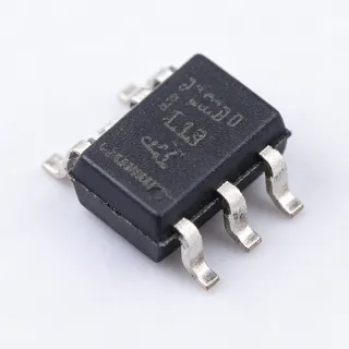
SN74AUP1T34QDCKRQ1 - AEC-Q100 1-Bit Level Translator | TI
MPN: SN74AUP1T34QDCKRQ1 ✓ Active| Qty | Unit Price | Extended |
|---|---|---|
| 1 | $0.42 | $0.42 |
| 10 | $0.38 | $3.80 |
| 100 | $0.32 | $32.00 |
| 500 | $0.28 | $140.00 |
| 1,000 | $0.25 | $250.00 |
SN74AUP1T34QDCKRQ1 Overview
A voltage-level translator (also called a level shifter) is a logic IC that interfaces digital signals between circuits operating at different supply voltages, for example connecting a 1.8V microcontroller output to a 3.3V peripheral input. Level translators sit within the broader logic IC family (buffers, translators, transceivers) and are essential wherever mixed-voltage domains coexist, which is nearly every modern embedded system.
Key features include two independent supply rails (VCCA and VCCB) that can each be set anywhere from 0.9V to 3.6V, allowing any-to-any translation between common logic levels such as 1.2V, 1.5V, 1.8V, 2.5V and 3.3V. The push-pull (non-inverting) output drives the signal actively in both directions, eliminating the need for external pull-up resistors required by open-drain solutions. The AUP (Advanced Ultra-low-Power) silicon technology delivers low dynamic power consumption, making the device attractive for battery-powered automotive and portable designs.
Architecturally, pin A is referenced to VCCA and receives the input signal, while pin B is referenced to VCCB and transmits the level-shifted output. Because both supplies support the same 0.9V to 3.6V range, the translator is direction-agnostic in voltage terms: it can translate low-to-high or high-to-low. TI controls the data sheet SN74AUP1T34-Q1, and the -Q1 suffix denotes AEC-Q100 automotive qualification including extended -40C to +125C operation.
Typical applications include automotive body electronics and ADAS sensor interfaces, I2C/SPI/UART signal translation between mixed-voltage ICs, GPIO level conversion in battery-powered portable equipment, and general-purpose 1-bit buffering in industrial control modules.
Design consideration: both VCCA and VCCB must be decoupled with 0.1uF ceramic capacitors placed close to pins 4 and 5, and the unused input should never be left floating since the AUP family inputs must be tied high or low.
This page adds value beyond the TI datasheet by synthesizing distributor pricing as of 2026-09-04, drop-in alternative analysis, and practical layout notes in one place.
Drop-in alternatives for SN74AUP1T34QDCKRQ1 — same package, pin-to-pin compatible. Different-package parts requiring PCB rework are excluded.
Variants in this series
Same-series models that are drop-in compatible with SN74AUP1T34QDCKRQ1 (same form factor and footprint) — differing in Output Type, Package.
Quick Comparison Tool — Select alternative parts for side-by-side comparison:
SN74AUP1T34DCKR
✅ Drop-In✓ In Stock
$0.09 / Unit
View Datasheet →SN74AUP1T34QDCKRQ1 Maximum Ratings & Electrical Characteristics
| Translator Type | Voltage Level |
| Channel Type | Unidirectional |
| Channels per Circuit | 1 |
| Output Type | Push-Pull, Non-Inverting |
| VCCA Supply Range | 0.9 V to 3.6 V |
| VCCB Supply Range | 0.9 V to 3.6 V |
| Logic Family | AUP (Advanced Ultra-low-Power) |
| Operating Temperature | -40C to +125C |
| Package | SC-70-5 (DCK) |
| Mounting Style | Surface Mount (SMD) |
| Qualification | AEC-Q100 (automotive) |
| Input Type | Single-ended, referenced to VCCA |
| Output Drive Referenced To | VCCB |
| Reel Packaging | Reel (DCKR) per manufacturer ordering code |
SN74AUP1T34QDCKRQ1 Pin Configuration
| Pin 1 | A — Input port referenced to VCCA |
| Pin 2 | GND — Ground |
| Pin 3 | B — Output port referenced to VCCB (non-inverting, push-pull) |
| Pin 4 | VCCB — Output-side supply, 0.9 V to 3.6 V |
| Pin 5 | VCCA — Input-side supply, 0.9 V to 3.6 V |
Typical Applications
SN74AUP1T34QDCKRQ1 is suitable for 6 applications: Automotive Body Electronics, Mixed-Voltage SPI/UART Interface Translation, Battery-Powered Portable Devices, Industrial Control and PLC I/O, Automotive Sensor Interfaces (ADAS), General-Purpose 1-Bit Logic Buffering.
Automotive Body Electronics
The SN74AUP1T34QDCKRQ1 is purpose-built for automotive body-control modules, door modules and lighting controllers where a -40C to +125C qualified translator bridges a low-voltage MCU domain (for example 1.8V) to a higher-voltage actuator or diagnostics domain (3.3V). Its AEC-Q100 qualification and Q1 suffix satisfy automotive PPAP supply-chain requirements, while the SC-70-5 package occupies under 3 mm of board area - valuable in dense body modules. Because the push-pull output actively drives both logic levels, no pull-up resistors are needed in the harness-side interface, reducing BOM count and improving edge rates. Decouple VCCA and VCCB each with 0.1uF ceramics near pins 4 and 5, and route the translated signal away from switch-node transients typical of automotive load drivers.
Recommended
Mixed-Voltage SPI/UART Interface Translation
In mixed-voltage boards where a 1.8V microcontroller communicates with 3.3V sensors, flash memories or radio modules, the SN74AUP1T34QDCKRQ1 provides single-bit point translation for SPI chip-select, UART TX, or clock lines. The dual 0.9V to 3.6V rails accept any common logic pair, and the AUP family's ultra-low dynamic power matters for always-on wake-up lines such as UART RX or interrupt signals that idle high. Because the device is unidirectional with a push-pull output, it preserves sharp edges without RC-slowing from pull-ups - important for clock lines above a few MHz. Place the translator physically close to the receiving IC and keep the two 0.1uF decoupling capacitors within 2 mm of pins 4 and 5 to minimize supply inductance and output ringing.
Recommended
Battery-Powered Portable Devices
The AUP (Advanced Ultra-low-Power) silicon technology of the SN74AUP1T34QDCKRQ1 makes it attractive for battery-operated wearables, meters and handheld instruments where every microamp on always-on signal paths counts. A single bit of level translation between a 1.2V or 1.8V low-power domain and a 3.3V peripheral draws minimal dynamic current, and the tiny SC-70-5 footprint supports compact PCB stacking. The wide 0.9V rail capability also tolerates low battery conditions better than 2.7V-minimum legacy translators, keeping interfaces valid as the cell discharges. For longest battery life, avoid translating high-frequency clocks unnecessarily and place the part close to its load to keep trace capacitance - and thus switching losses per edge - as low as possible.
Recommended
Industrial Control and PLC I/O
Industrial controllers routinely mix 1.8V or 2.5V FPGA/MCU banks with legacy 3.3V and 5V-tolerant field signals; the SN74AUP1T34QDCKRQ1 handles one such boundary per package with robust push-pull drive. Although this specific SKU is automotive-qualified, AEC-Q100 parts are commonly used in industrial designs for their margin and extended -40C to +125C range, which covers sealed control cabinets in hot environments. The non-inverting translation keeps firmware polarity assumptions unchanged when migrating boards between voltage generations. Designers should verify the receiver-side logic threshold is compatible with the VCCB-referenced output levels, and add a small series resistor (22 to 33 ohm) on long backplane traces to control reflections without unduly slowing the edge.
Recommended
Automotive Sensor Interfaces (ADAS)
ADAS sensor clusters - radar, ultrasonic, camera modules - generate low-voltage digital control and status signals inside a shielded module that must interface with 3.3V ECU logic. The SN74AUP1T34QDCKRQ1's AEC-Q100 qualification, -40C to +125C rating and push-pull output provide a deterministic, pull-up-free interface for one-wire status, enable, or interrupt signals crossing that boundary. The SC-70-5 package fits the tight module boards typical of sensor housings, and the dual independent rails allow the sensor-side domain and ECU-side domain to be decoupled from each other's supply sequencing at these pins. Keep the translated trace short and guarded from high-current harness run-throughs, and ensure both VCCA and VCCB ramp monotonically at startup to avoid undefined output states.
Recommended
General-Purpose 1-Bit Logic Buffering
Beyond level shifting, the SN74AUP1T34QDCKRQ1 works as a single-bit non-inverting buffer to restore degraded edges, isolate capacitive loading, or fan out one signal with fresh drive strength. Running VCCA and VCCB at the same voltage turns the part into a pure buffer; the push-pull AUP output delivers symmetric drive at both levels, outperforming weak MCU GPIOs that droop with heavy trace or connector capacitance. This is a common fix for long ribbon-cable runs, backplane stubs, and test-point-heavy prototypes. To preserve signal integrity, add a 22 to 33 ohm source-termination resistor at the buffer output for transmission lines longer than roughly one-sixth of the signal rise time, and keep the two 0.1uF supply decoupling capacitors tight to the package.
Recommended
Recommended Products Summary
Engineering reference data for SN74AUP1T34QDCKRQ1 — comparison, design guidance, and compliance information.
Selection Guide
Comparison with Alternatives
| Parameter | This Product | SN74AUP1T34DCKR |
|---|---|---|
| Package | SC-70-5 (DCK) | SC-70-5 (DCK) - same |
| Brand | Texas Instruments | Texas Instruments - same |
| Translator Type | 1-bit unidirectional, non-inverting | 1-bit unidirectional, non-inverting |
| VCCA Range | 0.9 V to 3.6 V | 0.9 V to 3.6 V |
| VCCB Range | 0.9 V to 3.6 V | 0.9 V to 3.6 V |
| Operating Temperature | -40C to +125C (AEC-Q100) | -40C to +125C (standard grade) |
| Automotive Qualification | Yes (AEC-Q100, Q1) | No |
| Output Type | Push-Pull, Non-Inverting | Push-Pull, Non-Inverting |
Key Differentiators
- AEC-Q100 automotive qualification (vs SN74AUP1T34DCKR)
- Ultra-low-power AUP silicon (vs Legacy 74LVC-family translators)
- Push-pull output removes pull-up resistors (vs Open-drain translator solutions)
Design Notes
Decouple both supply domains independently: place one 0.1uF ceramic capacitor within 2 mm of VCCA (pin 5) and another within 2 mm of VCCB (pin 4), each with a solid via to the respective ground plane. Because the SC-70-5 package has fine 0.5 mm pitch leads, verify the land pattern against the TI datasheet mechanical drawing before release. Connect GND (pin 2) directly to a low-impedance ground pour - the return current of the translated edge flows between VCCB and GND, so a fragmented ground increases output ringing.
The push-pull output drives sharp CMOS edges, so for traces longer than roughly one-sixth of the output rise time add a 22-33 ohm source-termination resistor at pin B. Do not add pull-up resistors - the output actively drives both levels and a pull-up only wastes current. Keep the input trace at pin A short and away from switching nodes; AUP inputs must never float, so tie any unused or gated inputs to VCCA or GND through a valid driver.
Two frequent mistakes: (1) swapping VCCA and VCCB - pin 4 is always the B-side supply and pin 5 the A-side supply; reversing them translates the level in the wrong direction or clamps the input. (2) Assuming bidirectionality - this is a fixed-direction translator (A to B only); for bidirectional buses use a -T45-type directional part instead. Also note both supplies must be within 0.9V to 3.6V at all times, including during power sequencing, to avoid undefined output states.
Compliance Information
AEC-Q100 qualification confirmed by the Q1 suffix and TI product documentation. RoHS/REACH/lead-free status not stated in the provided verified data; confirm on the TI product page for SN74AUP1T34.